Thermal Treatment for Reducing Transistor Performance Variation in Ferroelectric Memories

a ferroelectric memory and transistor technology, applied in the direction of capacitors, semiconductor devices, electrical apparatus, etc., can solve the problems of degrading the polarization characteristics of ferroelectric materials, essentially volatile devices, and loss of conventional mos capacitors' stored charge,

Active Publication Date: 2015-03-19
TEXAS INSTR INC
View PDF14 Cites 1 Cited by
  • Summary
  • Abstract
  • Description
  • Claims
  • Application Information

AI Technical Summary

Benefits of technology

[0015]Disclosed embodiments provide a method of manufacturing an integrated circuit including metal-oxide-semiconductor (MOS)

Problems solved by technology

As is fundamental in the art, however, those devices are essentially volatile, in that logic and memory circuits constructed according to these technologies do not retain their data states upon removal of bias power.
In contrast, conventional MOS capacitors lose their stored charge on power-down of the device.
However, it has been observed that this thermal treatment in a hydrogen-bearing atmosphere degrades the polarization characteristics of ferroelectric material 22, particularly for the case of PZT.
This deleterious effect necessitates omitting the hydrogen anneal thermal treatment from the conventional process flow in the manufacture of CMOS integrated circuits containing ferroelectric capacitors, such as FRAM integrated circuits.
The resulting variation in transistor electrical characteristics among a population of these devices as manufactured may require some yield loss to be tolerated, or may necess

Method used


Image

  • Thermal Treatment for Reducing Transistor Performance Variation in Ferroelectric Memories
  • Thermal Treatment for Reducing Transistor Performance Variation in Ferroelectric Memories
  • Thermal Treatment for Reducing Transistor Performance Variation in Ferroelectric Memories

Examples


Embodiment Construction

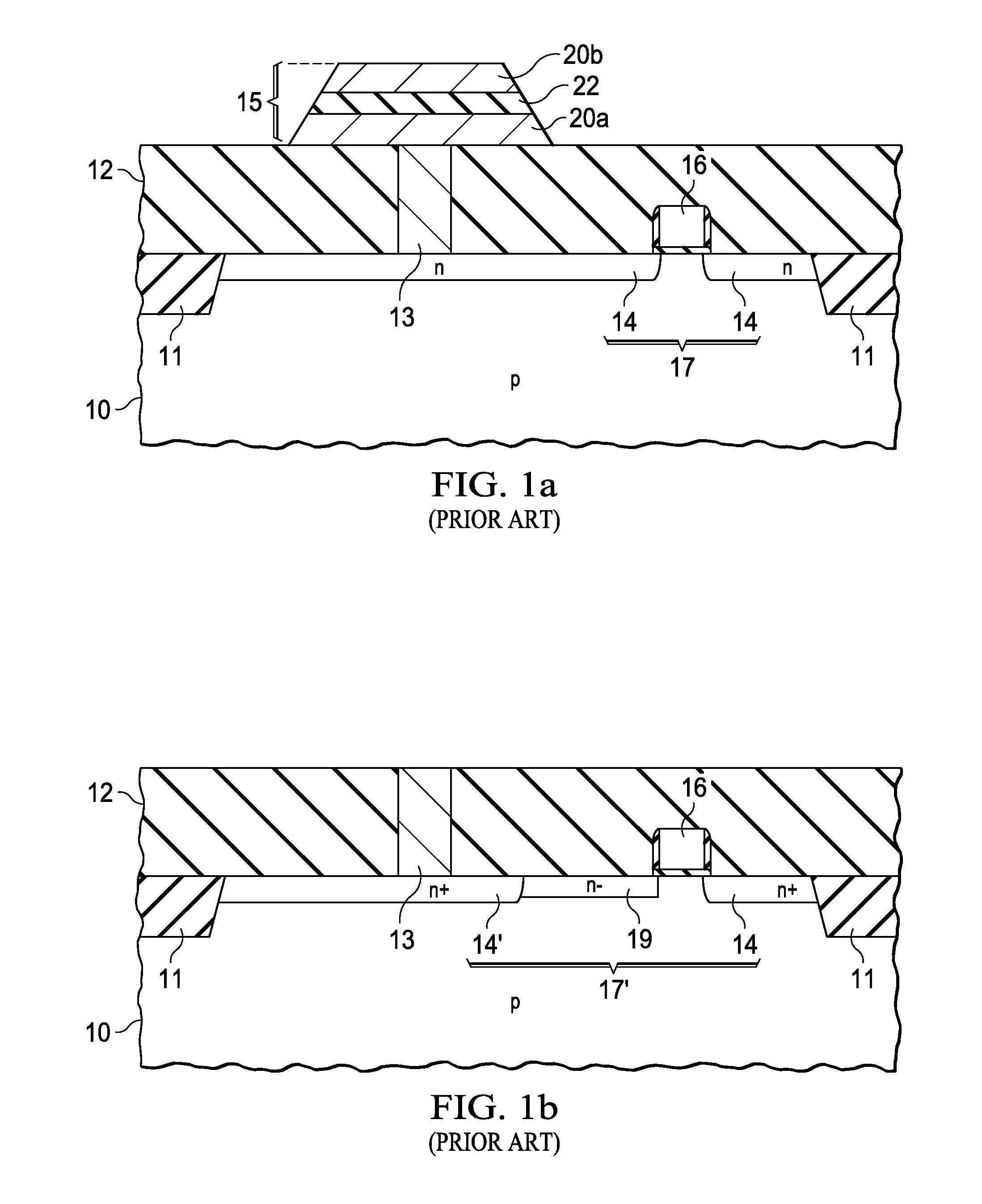
[0027]The one or more embodiments disclosed in this specification are described as implemented into the manufacture of semiconductor integrated circuits that include ferroelectric films, because it is contemplated that such implementation is particularly advantageous in that context. However, it is also contemplated that those skilled in the art having reference to this specification will recognize that concepts of this invention may be beneficially applied to other applications. Accordingly, it is to be understood that the following description is provided by way of example only, and is not intended to limit the true scope of this invention as claimed.

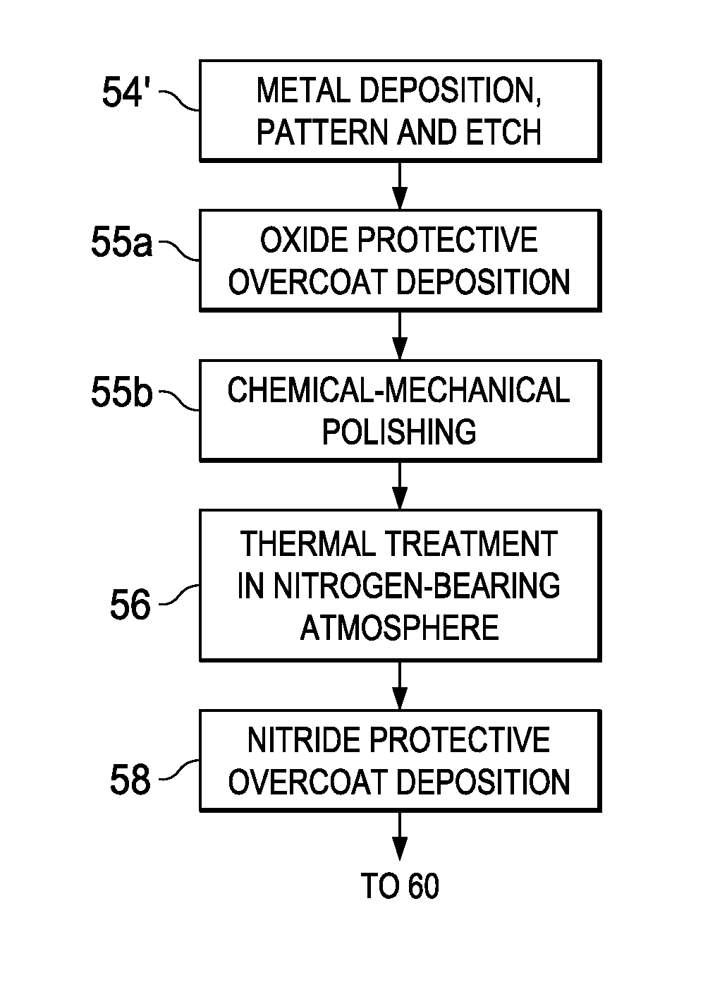
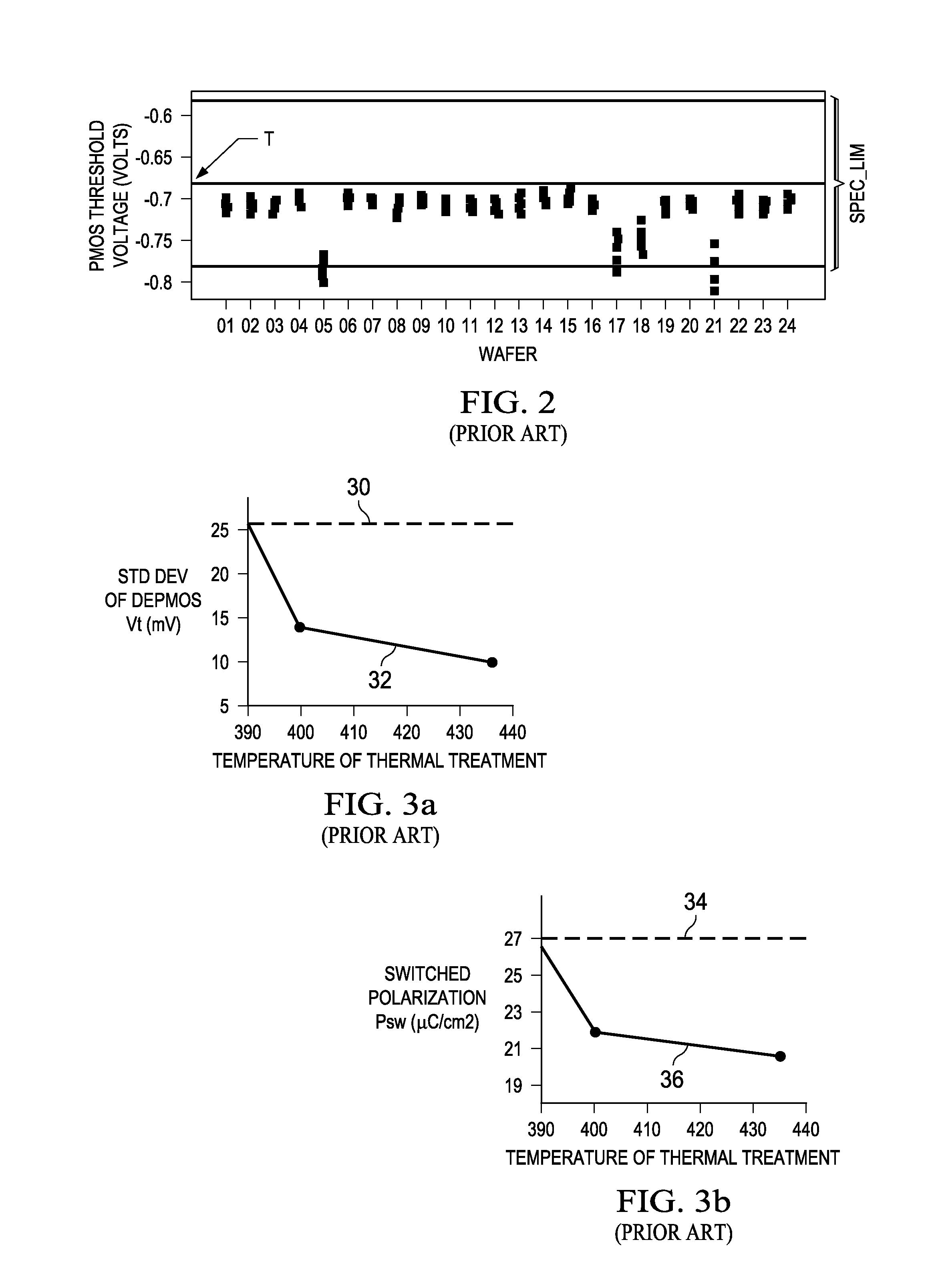
[0028]This description will refer to thermal treatment of semiconductor devices and wafers. Various terms in the art are commonly used to refer to such thermal treatment processes, including the terms “anneal” and “sinter”. For purposes of this description, we will use the term “thermal treatment” to refer to the treating of a semicon...


PUM


Abstract

Thermal treatment of a semiconductor wafer in the fabrication of integrated circuits including MOS transistors and ferroelectric capacitors, including those using lead-zirconium-titanate (PZT) ferroelectric material, to reduce variation in the electrical characteristics of the transistors. Thermal treatment of the wafer in a nitrogen-bearing atmosphere in which hydrogen is essentially absent is performed after formation of the transistors and capacitor. An optional thermal treatment of the wafer in a hydrogen-bearing atmosphere prior to deposition of the ferroelectric treatment may be performed.

Description

CROSS-REFERENCE TO RELATED APPLICATIONS[0001]This application claims priority, under 35 U.S.C. §119(e), of Provisional Application No. 61 / 878,117, filed Sep. 16, 2013, incorporated herein by this reference.STATEMENT REGARDING FEDERALLY SPONSORED RESEARCH OR DEVELOPMENT[0002]Not applicable.BACKGROUND OF THE INVENTION[0003]This invention is in the field of integrated circuit manufacture. Embodiments of this invention are more specifically directed to the formation of capacitors in memory devices such as ferroelectric memories.[0004]Conventional metal-oxide-semiconductor (MOS) and complementary MOS (CMOS) logic and memory devices are prevalent in modern electronic devices and systems, as they provide an excellent combination of fast switching times and low power dissipation, along with their high density and suitability for large-scale integration. As is fundamental in the art, however, those devices are essentially volatile, in that logic and memory circuits constructed according to t...

Claims


Application Information

Patent Timeline
IPC IPC(8): H01L27/115H01L29/66H01L21/324
CPCH01L27/11502H01L29/66477H01L21/324H01L28/57H01L29/66659H10B53/30
Inventor UDAYAKUMAR, KEZHAKKEDATH R.SAN, KEMAL TAMER
Owner TEXAS INSTR INC
Why Eureka
Try Eureka