Semiconductor switch circuit, signal processing apparatus, and ultrasound diagnostic apparatus

a switch circuit and switch technology, applied in the field of semiconductor switch circuits, signal processing apparatus, ultrasound diagnostic apparatus, can solve the problems of not being able to maintain the off isolation performance of the switch pair, and the danger of losing a function as a switch

Active Publication Date: 2015-03-26
HITACHI POWER SEMICON DEVICE
View PDF4 Cites 5 Cited by
  • Summary
  • Abstract
  • Description
  • Claims
  • Application Information

AI Technical Summary

Benefits of technology

[0025]A high breakdown voltage analog switch integrated circuit is required to have a low insertion loss, high breakdown voltage performance capable of withstanding a high voltage signal having positive and negative polarities, and off isolation performance (impedance in an OFF state) relative to a high frequency signal. Therefore, the high breakdown voltage analog switch integrated circuit of the comparative example needs the bias power supply 3 (refer to FIG. 5) that supplies the positive high voltage power supply VPP and the negative high voltage power supply VNN and has led to an inhibition factor to a size reduction and a reduction in power consumption.
[0032]Thus, since the signal processing apparatus does not need the positive or negative high voltage power supply which has been essential to the driving of the semiconductor switch circuit and the maintenance of the off isolation performance, its miniaturization and cost reduction are enabled. Reducing the high voltage circuit which has been required for the control of the electronic switch makes it easy to design a circuit board with its reduction and decreases a failure probability with a decrease in the number of components, thereby enhancing reliability of the signal processing apparatus.
[0034]Thus, since the ultrasound diagnostic apparatus does not need the positive or negative high voltage power supply which has been essential to the driving of the semiconductor switch circuit and the maintenance of the off isolation performance, its miniaturization and cost reduction are enabled. Reducing the high voltage circuit which has been required for control of the electronic switch makes it easy to design a substrate with its reduction and decreases a failure probability with a decrease in the number of components, thereby enhancing reliability of the ultrasound diagnostic apparatus.
[0036]According to the present invention, it is possible to provide a high breakdown voltage semiconductor switch circuit capable of being controlled by a low voltage power supply.

Problems solved by technology

Each of the MOSFETs 851 and 852 included in the switch pair 85 is not supplied with a sufficient on voltage due to an insertion loss and is in danger of losing a function as a switch in the worst case.
It is not possible to maintain the off isolation performance of the switch pair 85 in any case.

Method used


Image

  • Semiconductor switch circuit, signal processing apparatus, and ultrasound diagnostic apparatus
  • Semiconductor switch circuit, signal processing apparatus, and ultrasound diagnostic apparatus
  • Semiconductor switch circuit, signal processing apparatus, and ultrasound diagnostic apparatus

Examples


first embodiment

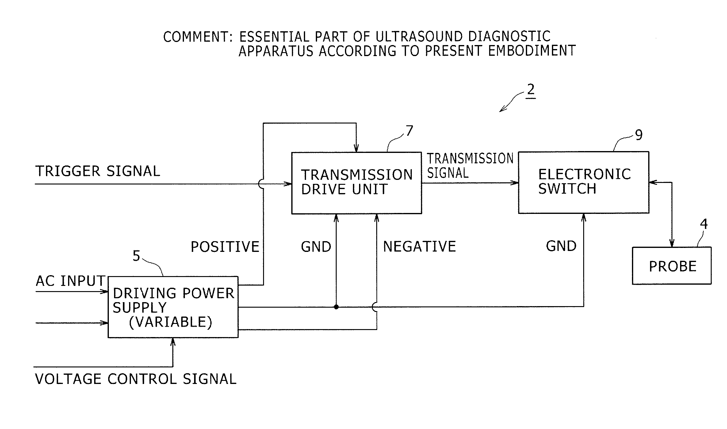
[0046]FIG. 1 is a configuration diagram showing an essential part of an ultrasound diagnostic apparatus 2 according to the present embodiment.

[0047]As shown in FIG. 1, the ultrasound diagnostic apparatus 2 of the present embodiment has a transmission drive unit 7 that generates a transmission signal based on a trigger signal, an electronic switch 9 that supplies the transmission signal to a probe 4, the probe 4 provided with a plurality of piezoelectric elements (not shown), and a driving power supply 5 that supplies a variable voltage.

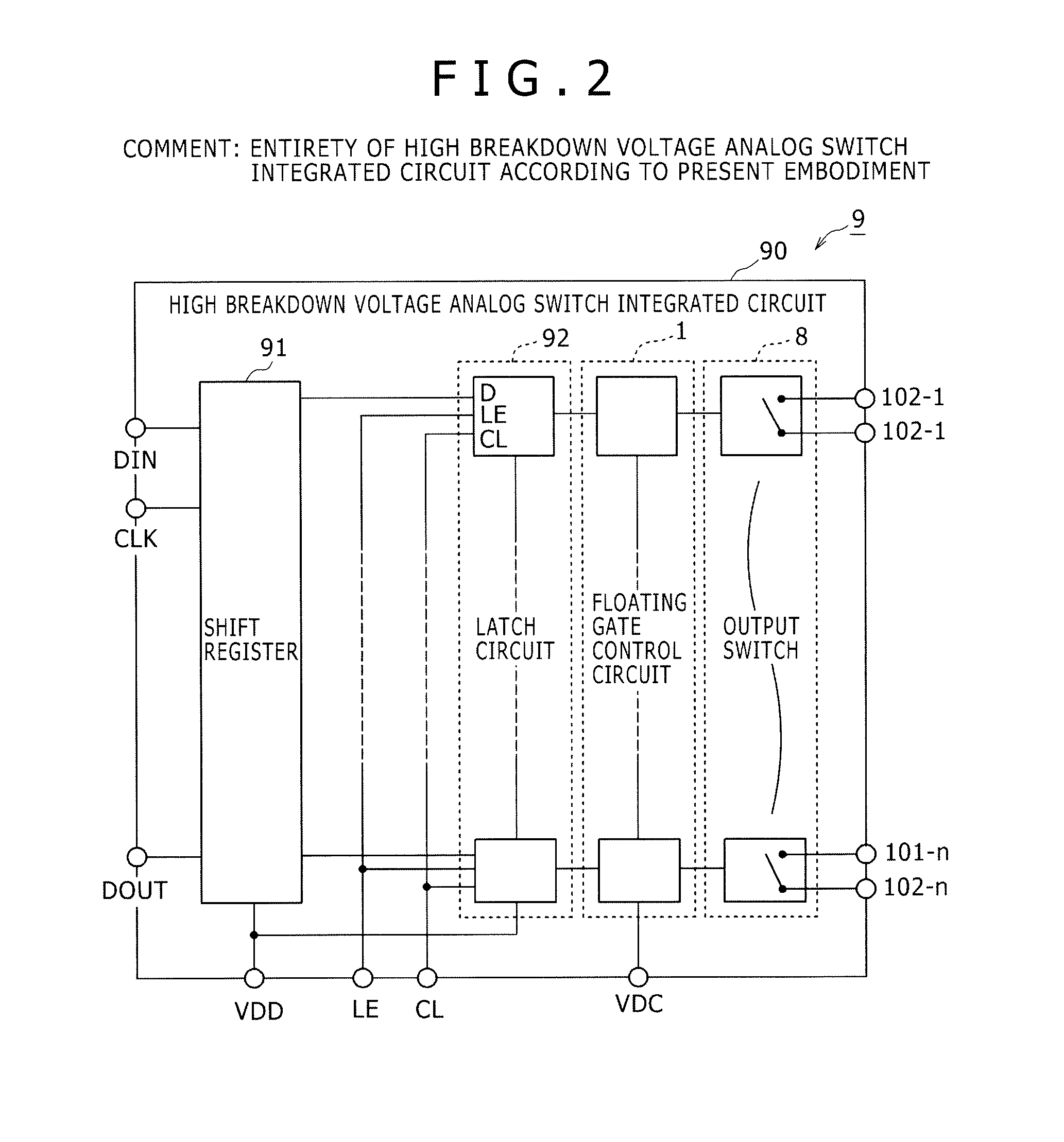
[0048]The electronic switch 9 is comprised of a semiconductor switch circuit. The electronic switch 9 in the present embodiment needs not to have the bias power supply 3 (refer to FIG. 5) which has been essential to the comparative example. Therefore, the application of a high breakdown voltage analog switch integrated circuit 90 of the present embodiment to the electronic switch 9 makes it unnecessary to provide the bias power supply 3 which has been...


PUM


Abstract

A semiconductor switch circuit comprises: a first switch pair including two MOSFETs having gates connected one another and sources connected to one another, and a zener diode reversely connected between the gates and sources of the MOSFETs; a second switch pair including two MOSFETs having gates connected one another and sources connected to one another, and a zener diode reversely connected between the gates and sources of the MOSFETs; and a third switch pair comprising two MOSFETs having gates connected to one another and sources connected to one another. The first switch pair and the second switch pair are connected in series between two input / output terminals through a connecting node. The third switch pair is connected to the connecting node between the first switch pair and the second switch pair.

Description

BACKGROUND OF THE INVENTION[0001]1. Field of the Invention[0002]The present invention relates to a semiconductor switch circuit equipped with a high breakdown voltage bidirectional analog switch, and a signal processing apparatus and an ultrasound diagnostic apparatus using the semiconductor switch circuit.[0003]2. Description of the Related Art[0004]There has recently been a demand for further miniaturization and decreasing in costs for an ultrasound diagnostic apparatus with its wider use. The ultrasound diagnostic apparatus has a piezoelectric probe for transmitting and receiving ultrasound, and a bidirectional analog switch for transmitting and receiving a drive signal of the piezoelectric probe and a signal of the ultrasound and further includes a plurality of power supplies for driving the bidirectional analog switch. A current ultrasound diagnostic apparatus is accompanied by a problem that the mounting of a plurality of power supplies becomes a bottleneck and a drastic size ...

Claims


Application Information

Patent Timeline
Patent Type & Authority Applications(United States)
IPC IPC(8): H03K17/10A61B8/00H03K17/687
CPCH03K17/102H03K2217/0009A61B8/4444H03K17/6871H03K17/063H03K17/0822H03K17/6874H03K2017/066H03K2217/0054
Inventor HONDA, HIRONOBUYAMASHITA, FUMIAKIAIZAWA, JUNICHI
Owner HITACHI POWER SEMICON DEVICE
Why Eureka
Try Eureka