Organic el display device

a display device and organic technology, applied in the direction of organic semiconductor devices, solid-state devices, thermoelectric devices, etc., can solve the problems of reducing the light emission efficiency, difficult high definition, and reducing the aperture ratio, so as to reduce the aperture ratio, reduce the precision of the vapor deposition process, and reduce the aperture ratio

Inactive Publication Date: 2015-04-02
JAPAN DISPLAY INC
View PDF2 Cites 4 Cited by
  • Summary
  • Abstract
  • Description
  • Claims
  • Application Information

AI Technical Summary

Benefits of technology

[0008]The organic EL display device that emits the light of each single color of RGB requires a vapor deposition mask and a vapor deposition process dedicated for the respective three colors of RGB in a manufacturing process. However, because a precision of the vapor deposition process is lower than a precision of a photolithography process, a space between pixels (accurately, between sub-pixels) must increase, to thereby make high definition difficult, and reduce an aperture ratio. As a result, there is a tendency to lower the light emission efficiency. Also, when white is extracted from tandem light emitting elements, light emitting layers are laminated on each other to increase a necessary voltage, and only a necessary single color is extracted from white by the color filters. As a result, the light emission efficiency decreases to prevent the low power consumption.

Problems solved by technology

However, because a precision of the vapor deposition process is lower than a precision of a photolithography process, a space between pixels (accurately, between sub-pixels) must increase, to thereby make high definition difficult, and reduce an aperture ratio.
As a result, there is a tendency to lower the light emission efficiency.

Method used


Image

  • Organic el display device
  • Organic el display device
  • Organic el display device

Examples


first embodiment

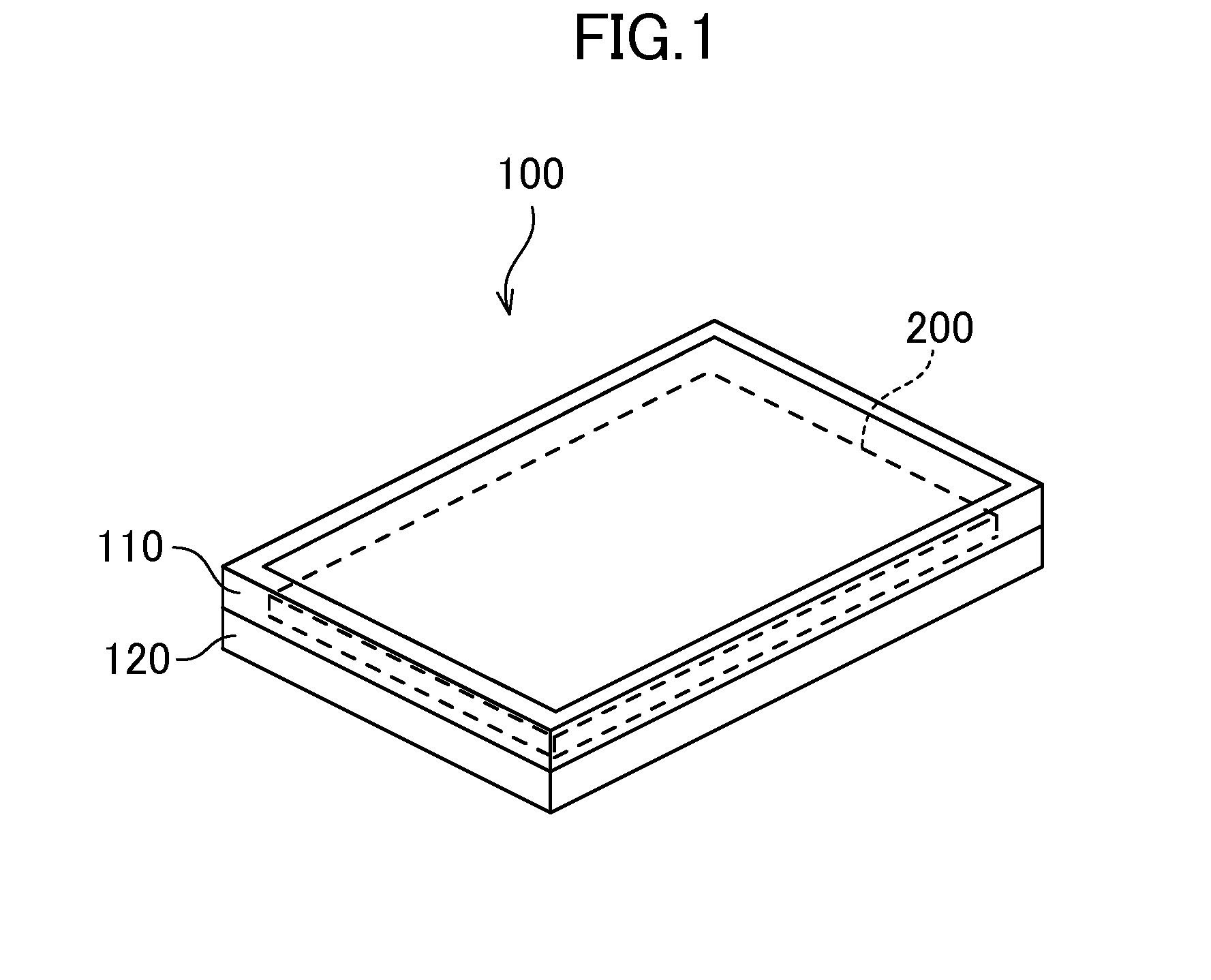
[0023]FIG. 1 schematically illustrates an organic EL display device 100 according to a first embodiment of the present invention. As illustrated in the figure, the organic EL display device 100 includes an organic EL panel 200 that is fixedly sandwiched between an upper frame 110 and a lower frame 120.

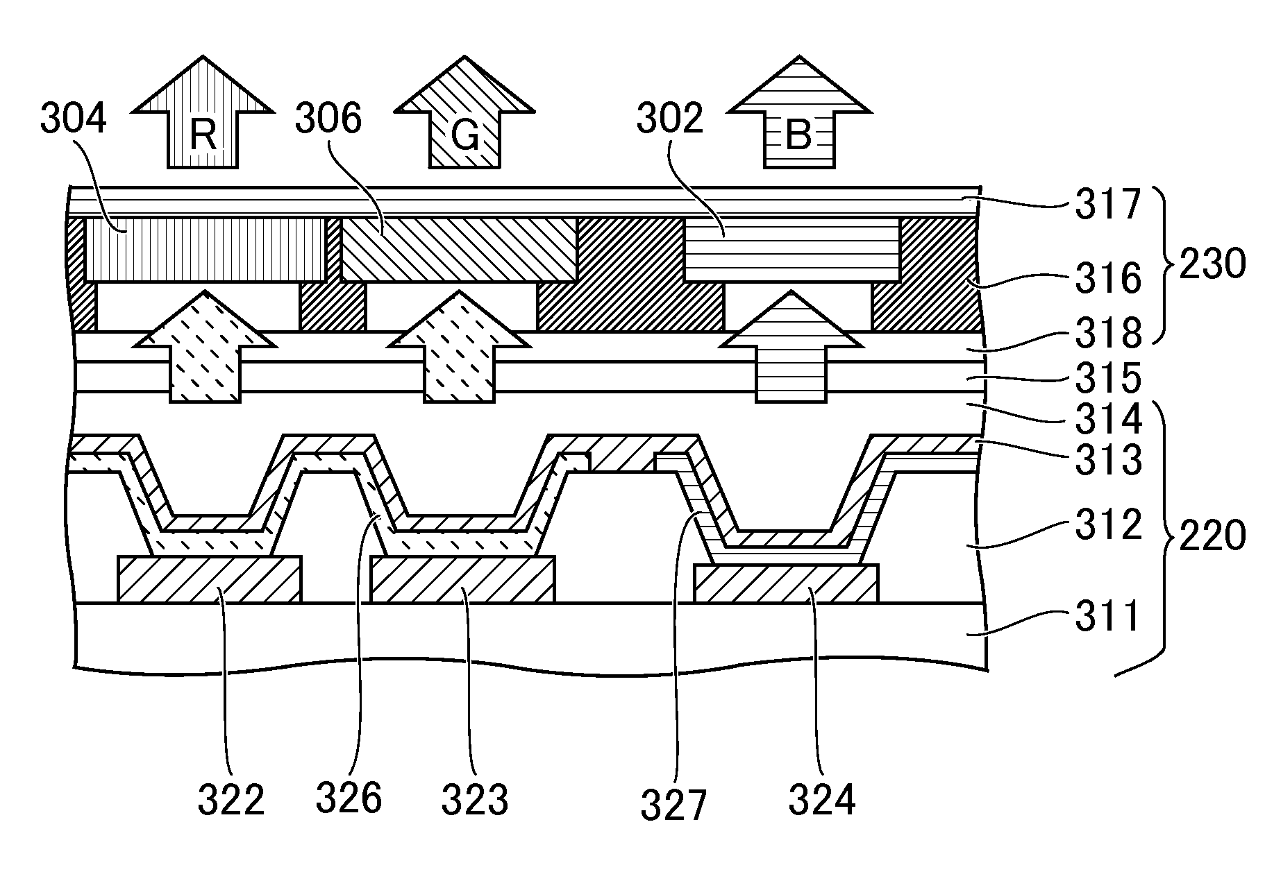
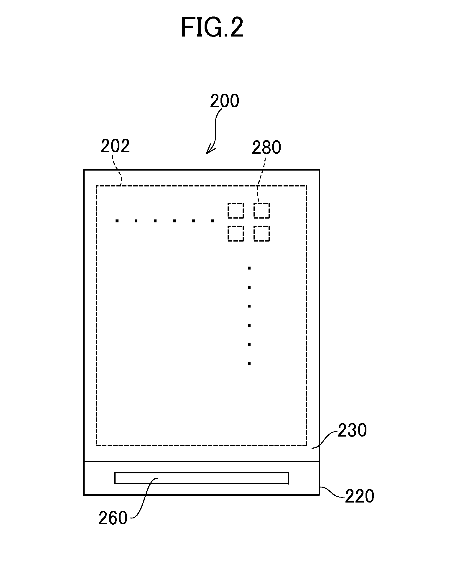
[0024]FIG. 2 illustrates a configuration of the organic EL panel 200 in FIG. 1. The organic EL panel 200 has two substrates of a TFT (thin film transistor) substrate 220, and a sealing substrate 230 that overlaps with the TFT substrate 220, and a space between those substrates is filled with a transparent resin 315 (refer to FIG. 4). The TFT substrate 220 has pixels 280 that are arranged in a display area 202 in a matrix. Also, on the TFT substrate 220 is placed a drive IC (integrated circuit) 260 that is a drive circuit which applies a potential for performing conduction between a source and a drain to scanning signal lines (not shown) of pixel transistors arranged in the respective p...

second embodiment

[0033]A description will be given of an organic EL display device according to a second embodiment of the present invention. An overall configuration of the organic EL display device according to the second embodiment is identical with that illustrated in FIGS. 1 and 2 of the first embodiment, and therefore a repetitive description will be omitted.

[0034]FIG. 6 is a diagram illustrating a layout of the first organic layer 326 and the second organic layer 327 in the TFT substrate 220 of the organic EL display device according to the second embodiment, in the same view as that in FIG. 5. As illustrated in FIG. 6, the organic EL display device according to the second embodiment is different from the organic EL display device according to the first embodiment in that an upper electrode contact hole 331 is formed.

[0035]When the upper electrode contact hole is to be formed in the organic EL panel where the organic layer is formed on the overall surface of the display area, there is a need ...


PUM


Abstract

An organic EL display device includes an organic layer having plural layers including a light emitting layer, and a color filter that passes a light of a predetermined wavelength region. The organic layer includes a first organic layer that is arranged in a first area having plural independent areas in a display area, and includes the light emitting layer that emits a light of a first wavelength region, and a second organic layer that is arranged in a second area having plural independent areas which is an area different from the first area in the display area, and includes the light emitting layer that emits a light of a second wavelength region which is different from the first wavelength region. The color filter has a first color filter and a second color filter that pass respective lights of different wavelength regions in the light emitted from the light emitting layer of the first organic layer.

Description

[0001]The present application claims priority from Japanese patent application JP2013-201401 filed on Sep. 27, 2013, the content of which is hereby incorporated by reference into this application.BACKGROUND OF THE INVENTION[0002]1. Field of the Invention[0003]The present invention relates to an organic EL display device.[0004]2. Description of the Related Art[0005]In recent years, an image display device (hereinafter referred to as “organic EL (electroluminescent) display device”) using a self-luminous body called “organic light emitting diode (OLED)” has been put in practical use. As compared with a related-art liquid crystal display device, because the organic EL display device uses a self-luminous body, the organic EL display device is not only excellent in visibility and response speed, but also does not require an auxiliary lighting device such as backlight. As a result, the organic EL display device can be further thinned.[0006]Color display in the organic EL display device of...

Claims


Application Information

Patent Timeline
Patent Type & Authority Applications(United States)
IPC IPC(8): H01L27/32H01L51/52
CPCH01L51/5203H01L27/322H10K59/35H10K59/38H10K50/824H10K2102/3026
Inventor UETAKE, NAOKI
Owner JAPAN DISPLAY INC
Why Eureka
Try Eureka