Method of fabricating semiconductor device structure

a semiconductor device and structure technology, applied in the field of semiconductor device structure fabrication, can solve the problem that the traditional mos transistor is difficult to scale down

Active Publication Date: 2015-04-02
UNITED MICROELECTRONICS CORP
View PDF11 Cites 6 Cited by
  • Summary
  • Abstract
  • Description
  • Claims
  • Application Information

AI Technical Summary

Benefits of technology

[0006]In view of the foregoing, this invention provides a method of fabricating a semiconductor device structure so as to prevent undercut from being formed in the gate dielectric layer under the gate electrode.

Problems solved by technology

The traditional MOS transistor is difficult to scale down due to the limitation of the fabricating process, and strained source / drain is therefore developed.

Method used


Image

  • Method of fabricating semiconductor device structure
  • Method of fabricating semiconductor device structure
  • Method of fabricating semiconductor device structure

Examples


Embodiment Construction

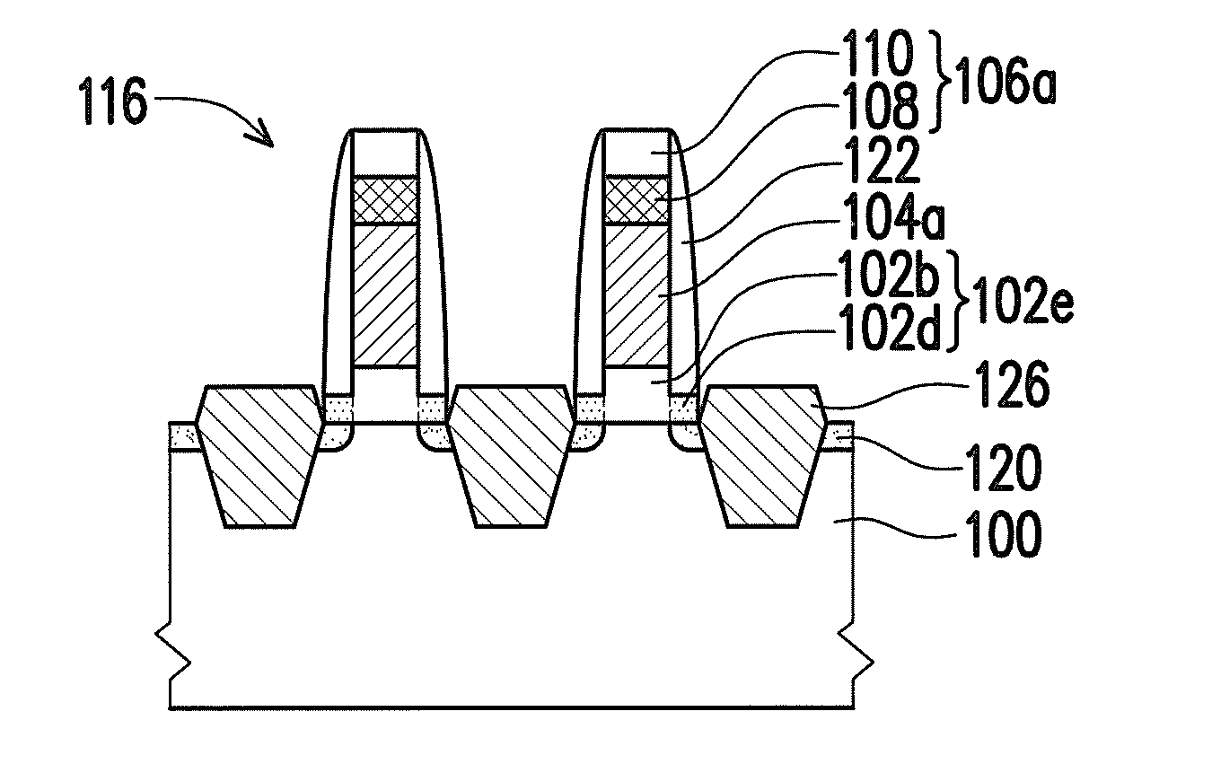
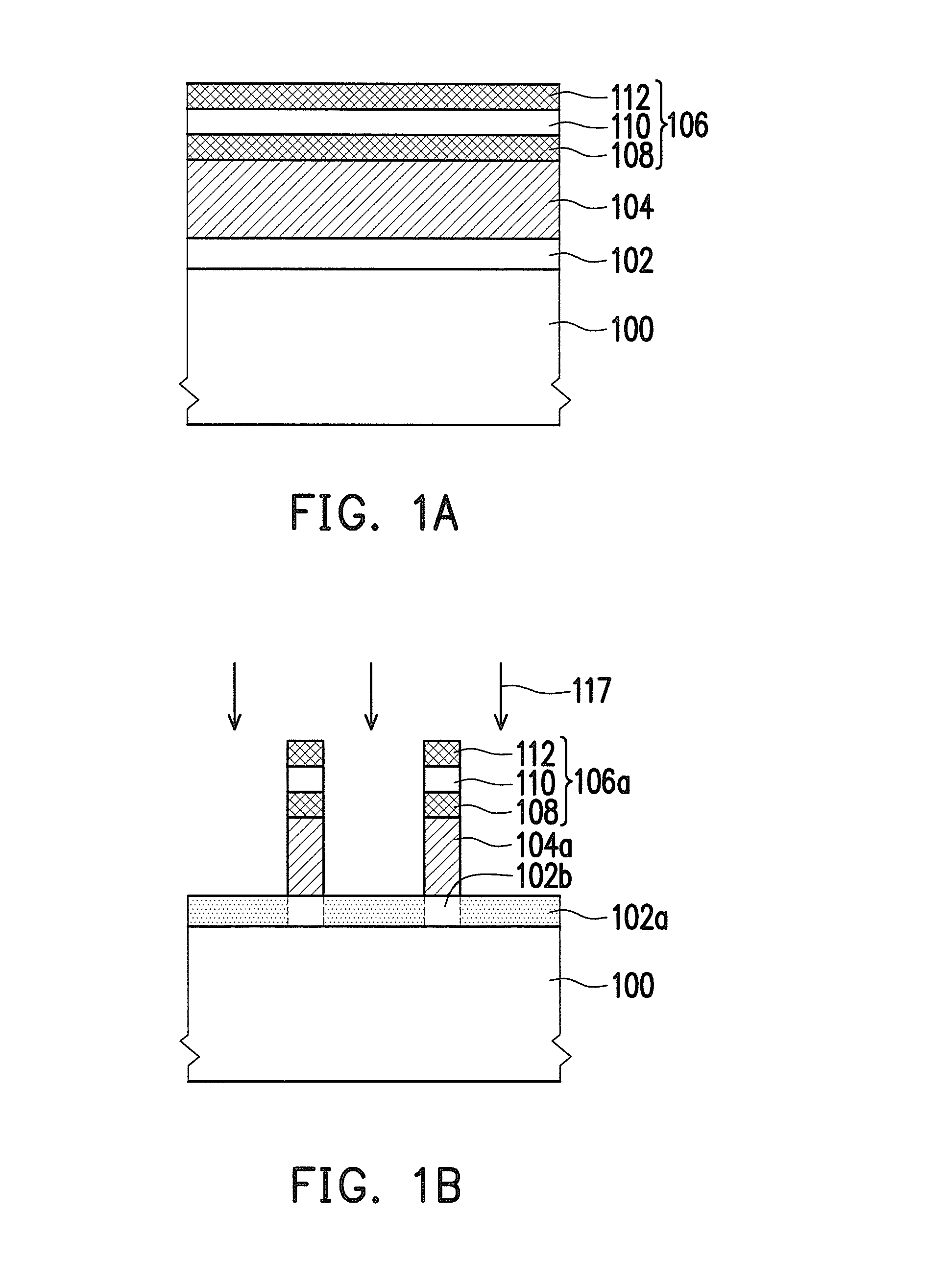
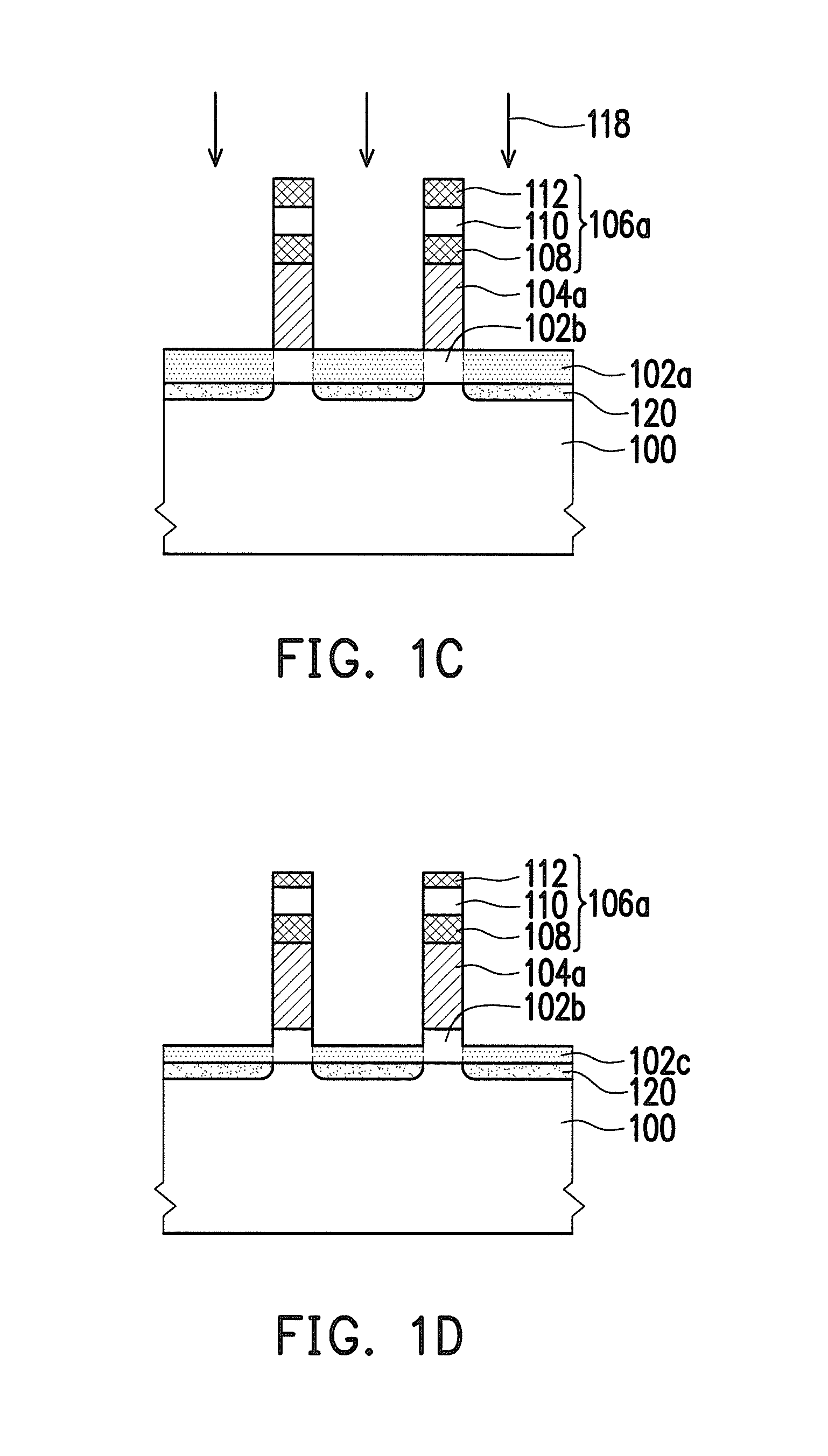
[0026]FIG. 1A to FIG. 1G are schematic cross-sectional views illustrating a method of forming a semiconductor device structure according to an embodiment of the present invention.

[0027]Referring to FIG. 1A, a substrate 100 is provided. The substrate 100 can be a semiconductor substrate, such as a silicon substrate. At least one shallow trench isolation (STI) structure (not shown) is formed in the substrate 100 for providing electrical isolation.

[0028]A gate dielectric layer 102 is formed on the surface of the substrate 100, and the gate dielectric layer 102 may include silicon oxide or silicon oxynitride, silicon nitride, or a high-k material (i.e. a dielectric material with a dielectric constant greater than 4). The high-k material can be metal oxide, such as rare earth metal oxide. The high-k material can be selected from the group consisting of hafnium oxide (HfO2), hafnium silicon oxide (HfSiO4), hafnium silicon oxynitride (HfSiON), aluminum oxide (Al2O3), lanthanum oxide (La2O3...


PUM


Abstract

A method of fabricating a semiconductor device structure is provided. The method includes the following step. A gate dielectric layer is formed on a substrate. A gate electrode is on the gate dielectric layer. The gate dielectric layer exposed by the gate electrode is treated. A first etching process is performed to remove at least a portion of the gate dielectric layer exposed by the gate electrode. A spacer is formed on the sidewall of the gate electrode. A second etching process is performed to form recesses in the substrate beside the gate electrode. Besides, during the first etching process and the second etching process, an etching rate of the treated gate dielectric layer is greater than an etching rate of the untreated gate dielectric layer.

Description

BACKGROUND OF THE INVENTION[0001]1. Field of Invention[0002]This invention is related to a semiconductor process, and particularly to a method of fabricating a semiconductor device structure.[0003]2. Description of Related Art[0004]MOS is a basic structure widely applied to various semiconductor devices, such as memory devices, image sensors and display devices. The traditional MOS transistor is difficult to scale down due to the limitation of the fabricating process, and strained source / drain is therefore developed. In the strained source / drain process, a single etching process is performed to form recesses beside the gate electrode, and a semiconductor compound having a lattice parameter different from that of the material of the substrate is grown in the recesses.[0005]However, since a longer time is required to etch the thick gate dielectric layer, the gate dielectric layer under the gate electrode may be etched in the lateral direction. Therefore, an undercut is observed in the...

Claims


Application Information

Patent Timeline
Patent Type & Authority Applications(United States)
IPC IPC(8): H01L21/28H01L21/311H01L29/66
CPCH01L21/28008H01L21/31111H01L29/66477H01L21/3086H01L21/31116H01L29/165H01L29/517H01L29/6659H01L29/66636H01L29/7834H01L29/7848
Inventor WU, YEN-LIANGCHANG, CHUNG-FUHUNG, YU-HSIANGFU, SSU-ILIN, CHIEN-TINGTZOU, SHIH-FANG
Owner UNITED MICROELECTRONICS CORP
Why Eureka
Try Eureka