Semiconductor devices including electrodes for temperature measurement

Active Publication Date: 2015-04-09
SAMSUNG ELECTRONICS CO LTD
View PDF11 Cites 12 Cited by
  • Summary
  • Abstract
  • Description
  • Claims
  • Application Information

AI Technical Summary

Benefits of technology

This patent improves the performance of circuits and predicts the reliability of semiconductor devices by measuring the temperature of conductive lines, which are elements of the devices. By measuring temperature close to the device, the accuracy of predicting its performance is improved. This is especially useful in preparing for temperature increases in the device.

Problems solved by technology

As a result, the temperature of the semiconductor device increases (self heating effect), and the performance of an original circuit design cannot be guaranteed.
As a result, the 3D structure is more affected by increases in temperature.
Although an apparatus having an additional temperature sensor is installed within the semiconductor device, the apparatus is relatively far from a position in which temperature should be measured, and thus, the temperature measurements are relatively imprecise.

Method used


Image

  • Semiconductor devices including electrodes for temperature measurement
  • Semiconductor devices including electrodes for temperature measurement
  • Semiconductor devices including electrodes for temperature measurement

Examples


Embodiment Construction

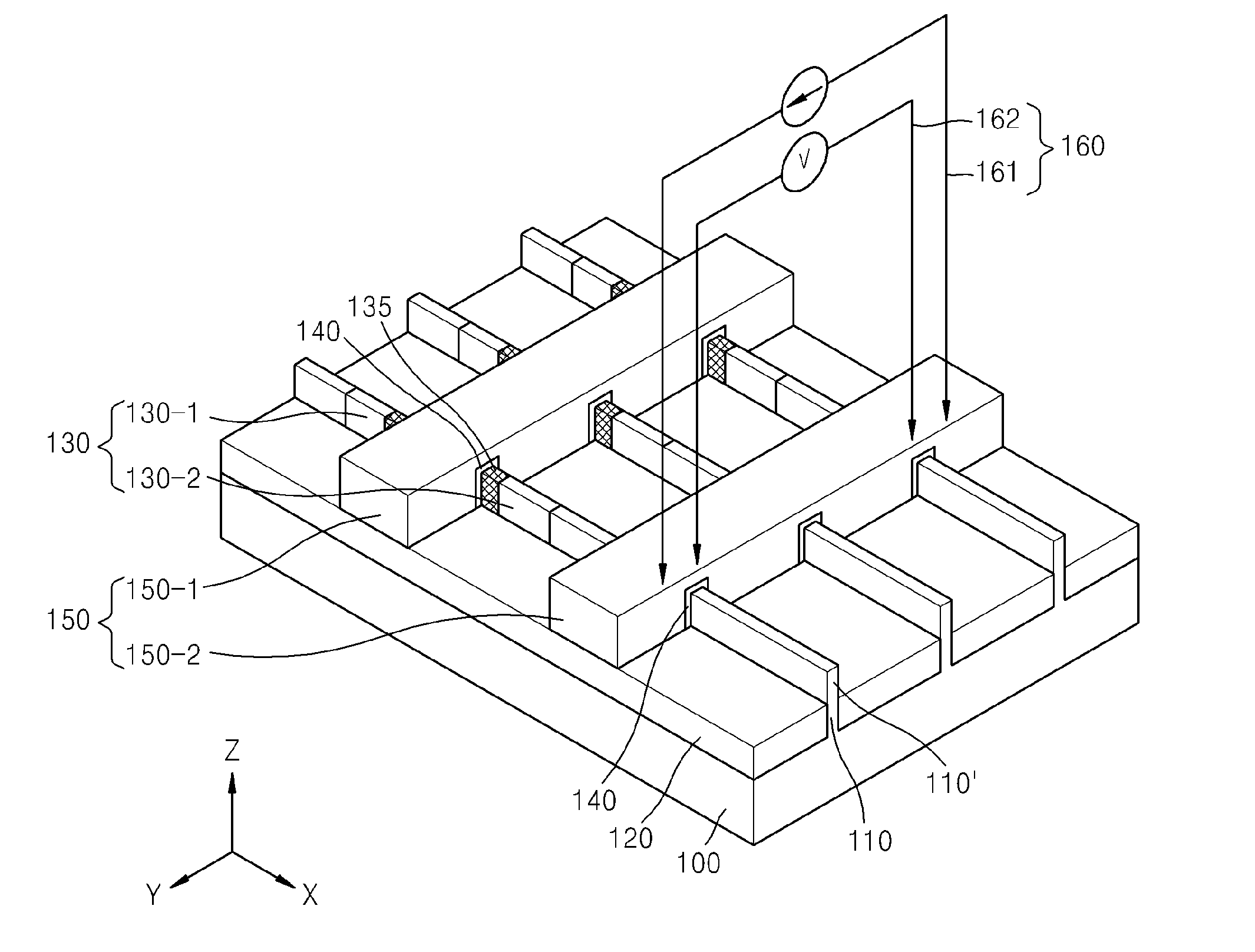
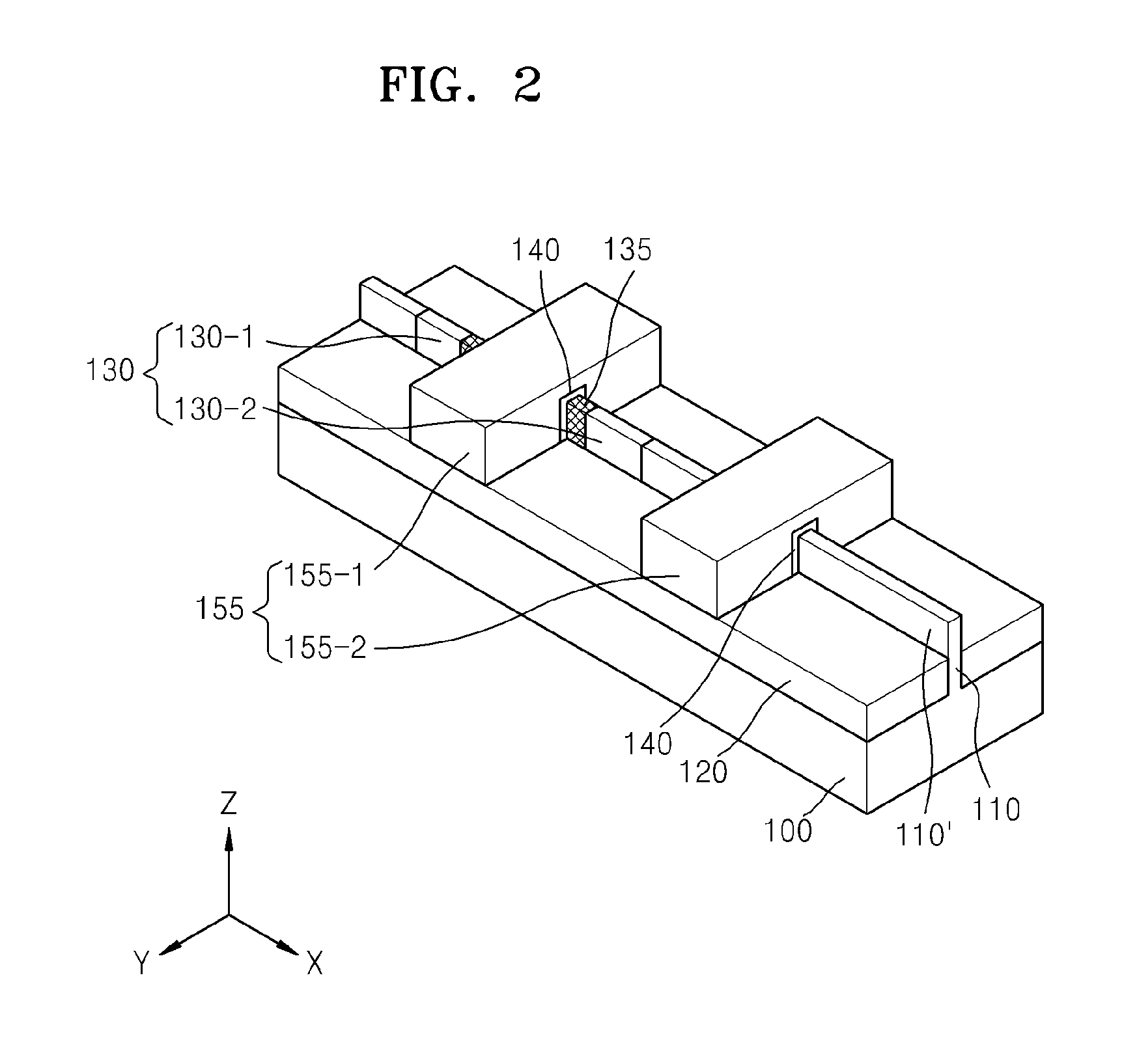
[0040]Example embodiments will now be described more fully with reference to the accompanying drawings. Inventive concepts may, however, be embodied in many different forms and should not be construed as being limited to the exemplary embodiments set forth herein; rather, these embodiments are provided so that this disclosure will be thorough and complete, and will fully convey the concept of the invention to those skilled in the art.

[0041]In the drawings, like reference numerals refer to like elements, and redundant descriptions thereof will be omitted. Furthermore, various elements and regions in the drawings are schematically drawn. Thus, the inventive concept is not limited by a relative size or distance drawn in the attached drawings.

[0042]It will be understood that, although the terms first and second etc. may be used herein to describe various elements, components, regions, layers and / or sections, these elements, components, regions, layers and / or sections should not be limit...


PUM


Abstract

A semiconductor device includes: a semiconductor substrate; a plurality of conductive lines formed on the semiconductor substrate; and an electrode for temperature measurement. The electrode is connected to the plurality of conductive lines. An electronic device includes a semiconductor device and has a temperature sensing function. The semiconductor device includes: a semiconductor substrate; a plurality of conductive lines formed on the semiconductor substrate; and an electrode for temperature measurement.

Description

CROSS-REFERENCE TO RELATED APPLICATIONS[0001]This application claims priority under 35 U.S.C. §119 to Korean Patent Application No. 10-2013-0119446, filed on Oct. 7, 2013, in the Korean Intellectual Property Office, the disclosure of which is incorporated herein in its entirety by reference.BACKGROUND[0002]1. Field[0003]Example embodiments of inventive concepts relate to semiconductor devices, and more particularly, to semiconductor devices that may more precisely measure temperature of semiconductor devices, and / or electronic devices including the same.[0004]2. Description of Related Art[0005]As semiconductor devices become more highly integrated, heat generated when a semiconductor device is driven is not dissipated outside of the semiconductor device. As a result, the temperature of the semiconductor device increases (self heating effect), and the performance of an original circuit design cannot be guaranteed. For example, although a three-dimensional (3D) structure, such as FinF...

Claims


Application Information

Patent Timeline
IPC IPC(8): G01K7/01H01L23/34H01L29/78H01L29/41
CPCG01K7/01H01L29/785H01L23/34H01L29/41B82Y40/00H01L27/0886H01L29/0673H01L29/775H01L2924/0002H01L2924/00H01L21/28H01L22/00
Inventor LEE, KYONGTAEKPAE, SANGWOOPARK, JUNEKYUN
Owner SAMSUNG ELECTRONICS CO LTD
Why Eureka
Try Eureka