Method and system for mounting circuit design on reconfigurable device

Inactive Publication Date: 2010-01-21
FUJIFILM BUSINESS INNOVATION CORP
View PDF7 Cites 21 Cited by
  • Summary
  • Abstract
  • Description
  • Claims
  • Application Information

AI Technical Summary

Benefits of technology

[0019]Yet another aspect of the present invention is a program or a program product for causing a computer to generate configuration data for reconfiguring a reconfigurable device. The program product includes preparing hardware information including definition data for the plurality of processing elements included in the respective groups and definition data for the routing matrix on a database that the computer can access to. The program also includes mapping a circuit design onto the plural

Problems solved by technology

The method of mapping also comprises changing node assignment of the first node from a current location to a different location without changing node assignment of at least one other node in the first CLB and such change in node assignment results in a change of circuit performance.
In a reconfigurable device that includes a PLD such as an FPGA (Field Programmable Gate Array),

Method used


Image

  • Method and system for mounting circuit design on reconfigurable device
  • Method and system for mounting circuit design on reconfigurable device
  • Method and system for mounting circuit design on reconfigurable device

Examples


Embodiment Construction

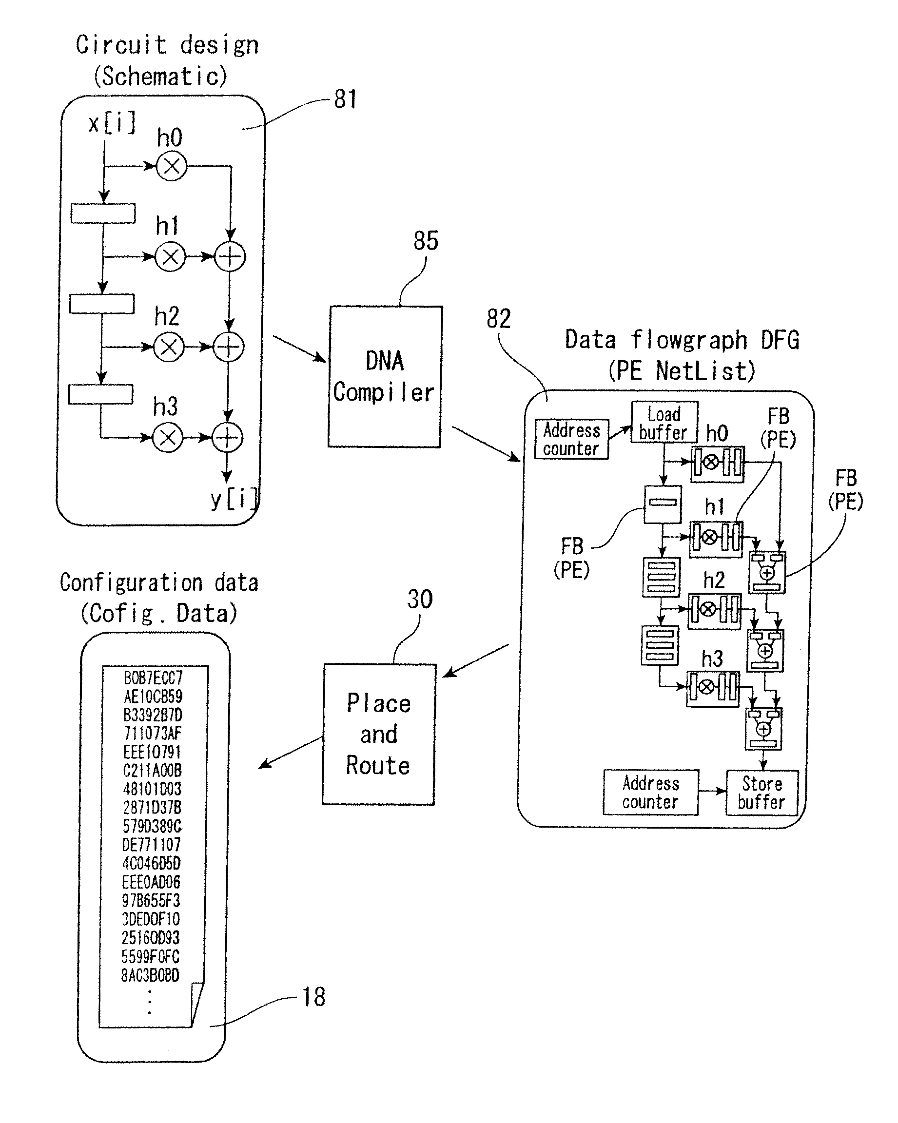
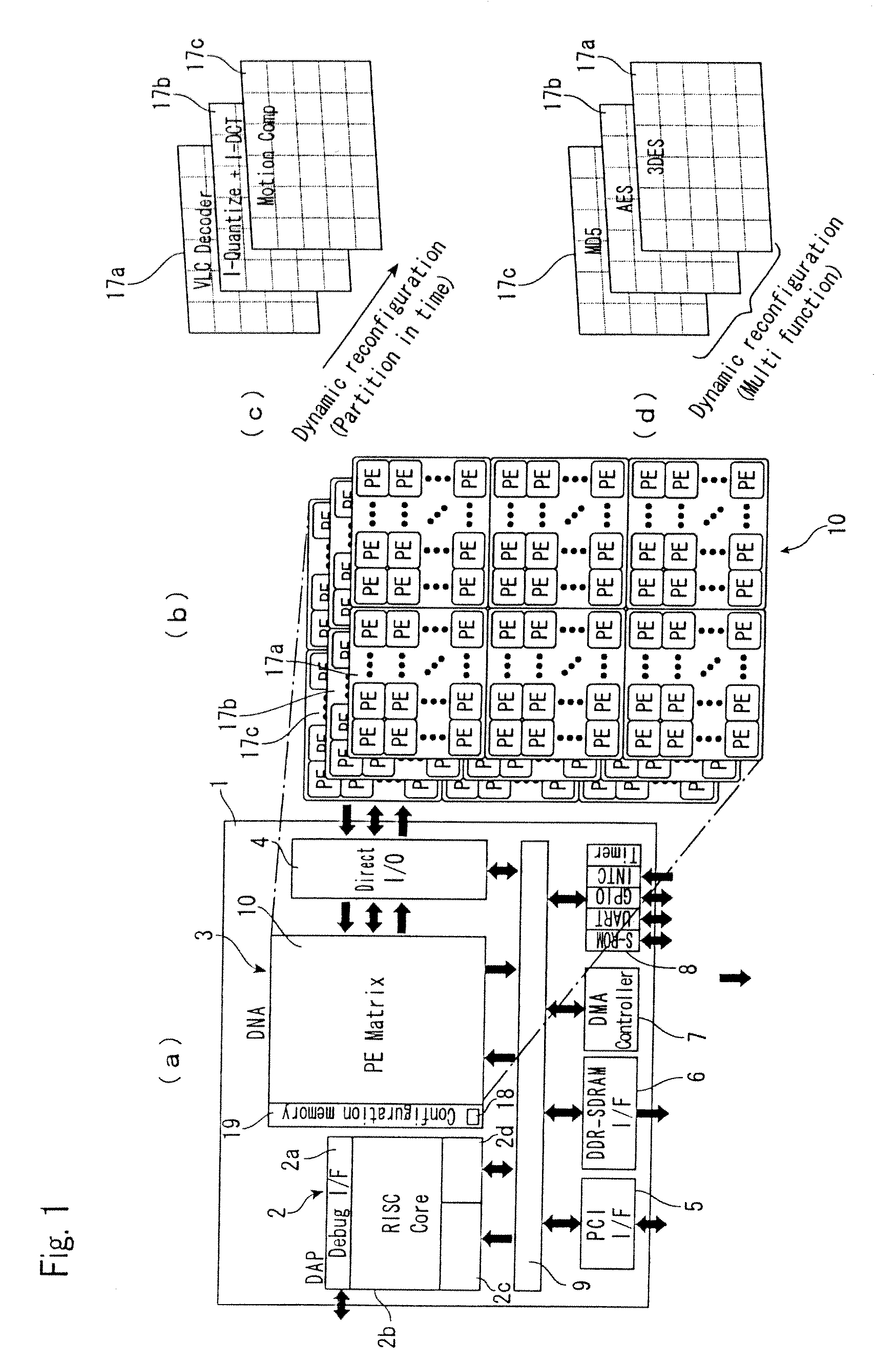
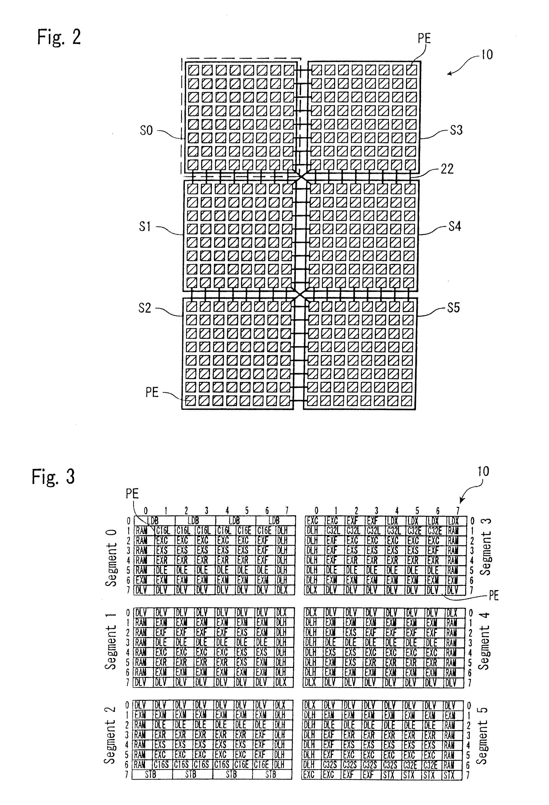
[0043]FIG. 1(a) shows one example of a reconfigurable device. This device 1 is a semiconductor integrated circuit device called a “DAPDNA” that has been developed by the present applicant. The device 1 includes a RISC core module 2 called a “DAP” and a dynamic reconfigurable data-flow accelerator 3 called a “DNA”. In addition to the DAP 2 and the DNA 3, the device 1 includes an interface 4 for direct input / output to the DNA 3, a PCI interface 5, an SDRAM interface 6, a DMA controller 7, other peripheral devices 8, and a high-speed switching bus 9 for connecting such elements. The DAP 2 includes a debugging interface 2a, a RISC core 2b, an instruction cache 2c, and a data cache 2d. The DNA 3 includes a PE matrix 10 where 376 processing elements PE (hereinafter simply referred to as “PE” or “PEs”) are placed in two dimensions and a configuration memory 19 that stores configuration data 18 for reconfiguring the PE matrix 10 by changing the functions of the plurality of processing eleme...


PUM


Abstract

There is provided a system for generating configuration data for implementing a circuit design in a segmented reconfigurable device. A placement and routing design aiding system (30) includes a database (31) for storing hardware information (89) including data of PEs included in each segment and data of a first-level and second-level routing matrix and an apparatus (33) for mapping the circuit design onto the PEs. The mapping apparatus (33) generates mappings of the circuit design onto the PEs by carrying out an iterative algorithm that minimizes a cost function based on the hardware information (89). The cost function includes an item that minimizes usage of the second-level routing matrix (22) that connects between the segments.

Description

FIELD OF THE INVENTION[0001]The present invention relates to a method and system for implementing a desired circuit design in a device in which circuits can be reconfigured.RELATED ART[0002]Japanese Laid-Open Patent Publication No. 2000-200298 discloses an automatic placement method that is characterized by storing circuit data, which is composed of a component list and a net list, and placement data for the circuit data in a database, converting new circuit data and circuit data in the database respectively to graphs composed of nodes and edges, matching the converted graphs with one another to find circuit data with a high degree of matching, and placing the new circuit data in accordance with placement data that is paired with the circuit data found by the matching. The publication states that simulated annealing, a neural network, mean field annealing, or a genetic algorithm is used when placing the new circuit in accordance with the placement data paired with the circuit data t...

Claims


Application Information

Patent Timeline
IPC IPC(8): G06F17/50
CPCH03K19/17736G06F30/34G06F30/39G06F30/347
Inventor BACHINA, SATISHMURTHY, PRAKASH SREEDHARKANNAN, VANAMAMALAIHEGDE, VINAY CHIDAMBARKIMURA, HIROYUKI
Owner FUJIFILM BUSINESS INNOVATION CORP
Why Eureka
Try Eureka