Wafer processing method

Active Publication Date: 2015-04-16
DISCO CORP
View PDF0 Cites 13 Cited by
  • Summary
  • Abstract
  • Description
  • Claims
  • Application Information

AI Technical Summary

Benefits of technology

[0016]In the functional layer removing step of the wafer processing method according to the present invention, the CO2 laser beam is applied to the wafer along each division line in the condition where the spot of the CO2 laser beam having a width corresponding to the width of each division line is set on the upper surface of each division line, thereby removing the functional layer along each division line. The functional layer can be removed along each division line by one stroke of application of the CO2 laser beam having a high power, thereby improving the productivity.
[0017]In the

Problems solved by technology

However, when the wafer is cut by the cutting blade in the condition where the cutting blade is positioned at the lateral center between the two laser processed grooves, there arises a new problem such that the cutting blade may meander so as to be caught by the two laser processed grooves as in the case that a tire is caug

Method used


Image

  • Wafer processing method
  • Wafer processing method
  • Wafer processing method

Examples


Example

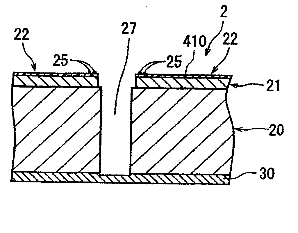
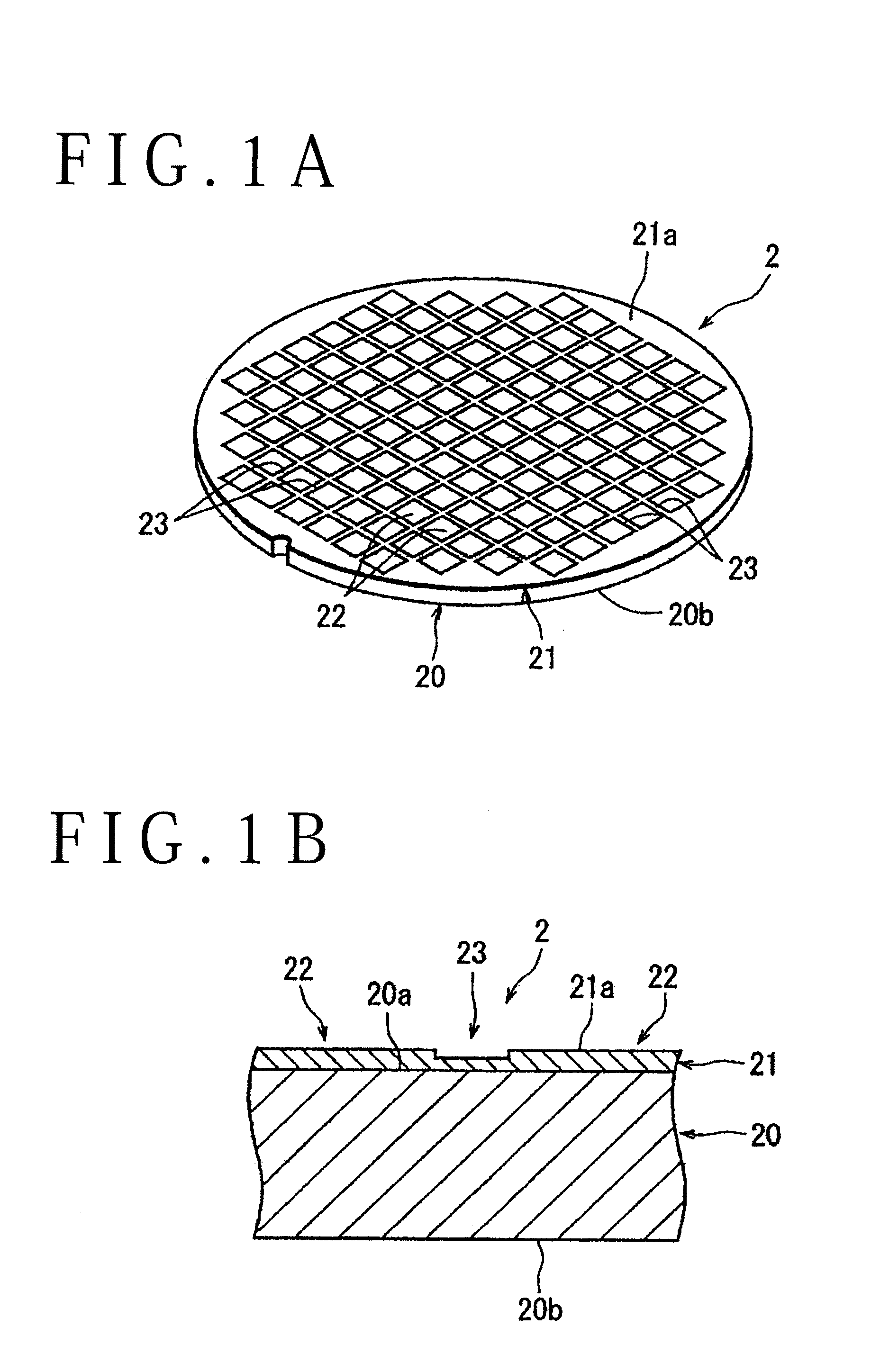
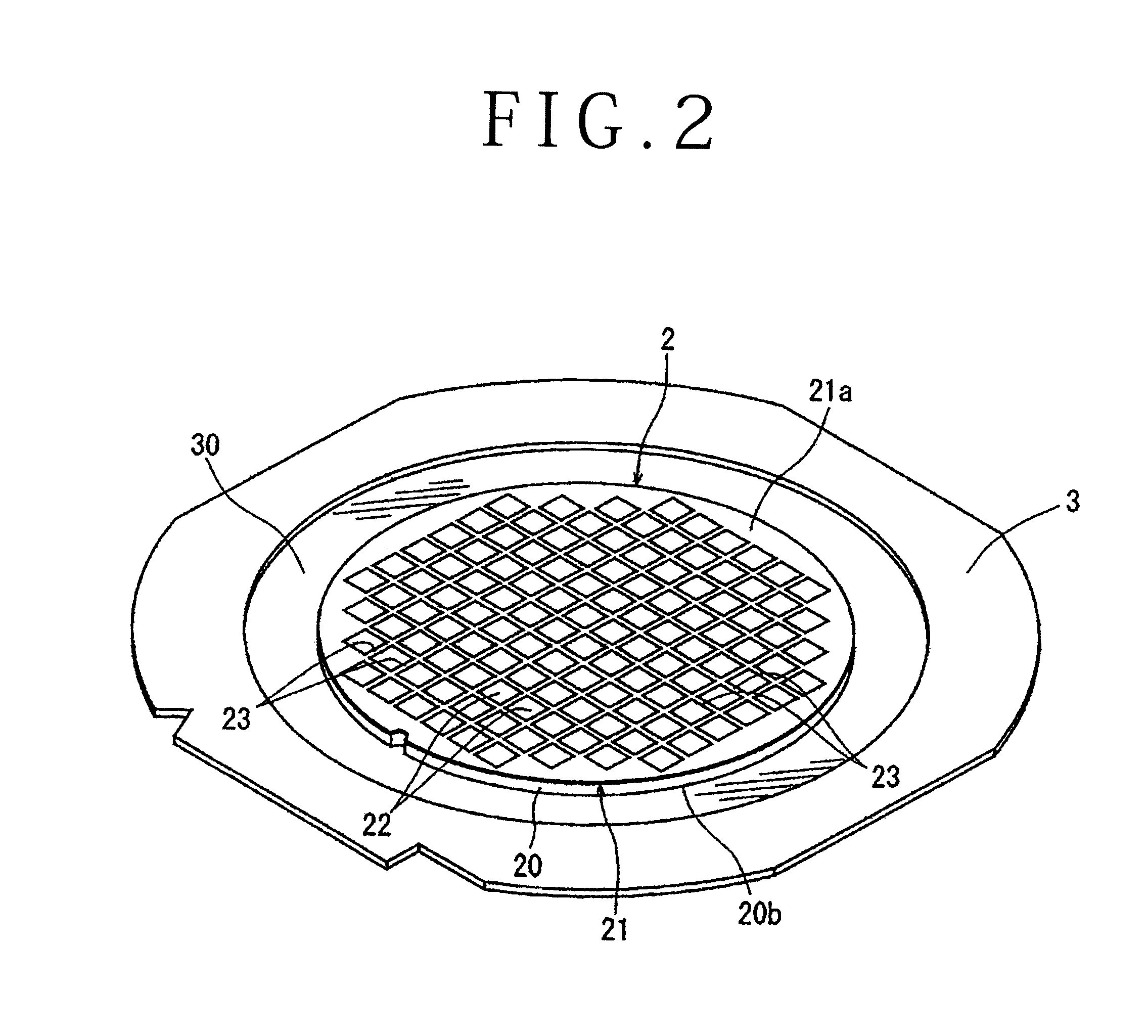
[0032]The wafer processing method according to the present invention will now be described in more detail with reference to the attached drawings. FIG. 1A is a perspective view of a semiconductor wafer 2 to be divided into individual devices by the wafer processing method according to the present invention, and FIG. 1B is an enlarged sectional view of an essential part of the semiconductor wafer 2 shown in FIG. 1A. As shown in FIGS. 1A and 1B, the semiconductor wafer 2 is composed of a substrate 20 such as a silicon substrate and a functional layer 21 formed on the front side 20a of the substrate 20. For example, the substrate 20 has a thickness of 150 μm. The functional layer 21 is composed of an insulating film and a functional film formed on the insulating film, the functional film forming a plurality of circuits. A plurality of devices 22 such as ICs and LSIs are formed like a matrix from the functional layer 21. These devices 22 are partitioned by a plurality of crossing divisi...


PUM


Abstract

A wafer processing method divides a wafer into a plurality of individual devices along a plurality of crossing division lines formed on the front side of the wafer. The method includes a functional layer removing step of applying a CO2 laser beam to the wafer along each division line with the spot of the CO2 laser beam, having a width corresponding to the width of each division line set on the upper surface of each division line, thereby removing a functional layer along each division line to form a groove along each division line where the functional layer has been removed, and a groove shaping and debris removing step of applying a laser beam having a wavelength in the ultraviolet region to the wafer along each groove, thereby removing debris sticking to the bottom surface of each groove and also shaping the side walls of each groove.

Description

BACKGROUND OF THE INVENTION[0001]1. Field of the Invention[0002]The present invention relates to a wafer processing method for dividing a wafer into a plurality of individual devices along a plurality of crossing division lines formed on the front side of the wafer, the wafer including a substrate such as a silicon substrate and a functional layer formed on the front side of the substrate, the individual devices being formed from the functional layer and partitioned by the division lines.[0003]2. Description of the Related Art[0004]As well known in the art, in a semiconductor device fabrication process, a functional layer composed of an insulating film and a functional film is formed on the front side of a substrate such as a silicon substrate, and a plurality of devices such as ICs and LSIs are formed like a matrix from this functional layer, thus obtaining a semiconductor wafer having the plural devices. The plural devices are partitioned by a plurality of division lines formed on...

Claims


Application Information

Patent Timeline
IPC IPC(8): H01L21/78H01L21/683
CPCH01L21/78H01L21/6836H01L2221/68327H01L21/268
Inventor AIKAWA, CHIKARATAKAHASHI, KUNIMITSUKITAHARA, NOBUYASUFUJIWARA, SEIJIYODO, YOSHIAKIKUKI, JUNICHI
Owner DISCO CORP
Why Eureka
Try Eureka