Variable matching circuit and amplifier

Inactive Publication Date: 2015-04-30
PANASONIC CORP
View PDF1 Cites 10 Cited by
  • Summary
  • Abstract
  • Description
  • Claims
  • Application Information

AI Technical Summary

Benefits of technology

[0020]According to the present disclosure, it is possible to reduce a loss in an input high frequency signal, to change a gain, and to reduce reflection of the h

Problems solved by technology

For example, when the low noise amplifier has the variable gain function, performance degradation of the low noise amplifier remarkably appears, resulting in performance degradation of the receiver.
For

Method used


Image

  • Variable matching circuit and amplifier
  • Variable matching circuit and amplifier
  • Variable matching circuit and amplifier

Examples


first embodiment

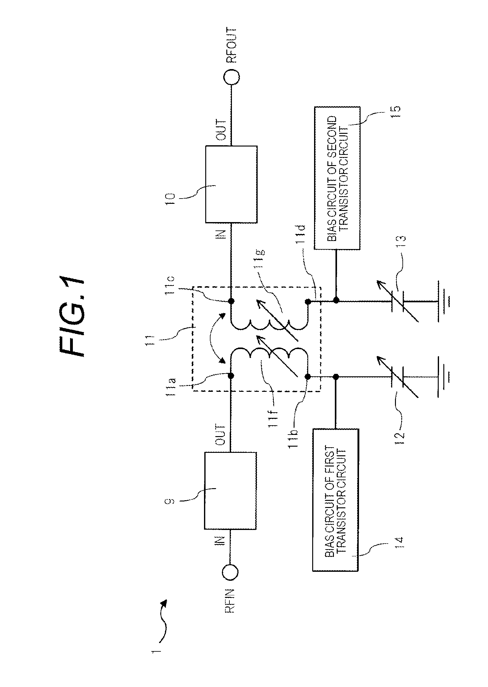
[0048]FIG. 1 is a diagram illustrating an internal configuration of a variable matching circuit 1 according to a first embodiment. The variable matching circuit 1 illustrated in FIG. 1 includes a first transistor circuit 9, a second transistor circuit 10, a transformer 11, a first capacitive element 12, and a second capacitive element 13. Furthermore, the variable matching circuit 1 may further include a bias circuit 14 for the first transistor circuit, and a bias circuit 15 for the second transistor circuit.

[0049]The first transistor circuit 9 is operated by a DC power source voltage supplied from the bias circuit 14 for the first transistor circuit, amplifies a high frequency signal input to an input terminal RFIN, and outputs the signal to a primary inductor device 11f of the transformer 11.

[0050]The second transistor circuit 10 is operated by a DC power source voltage supplied from a power source voltage generating circuit (not illustrated), and the high frequency signal amplifi...

modification example of first embodiment

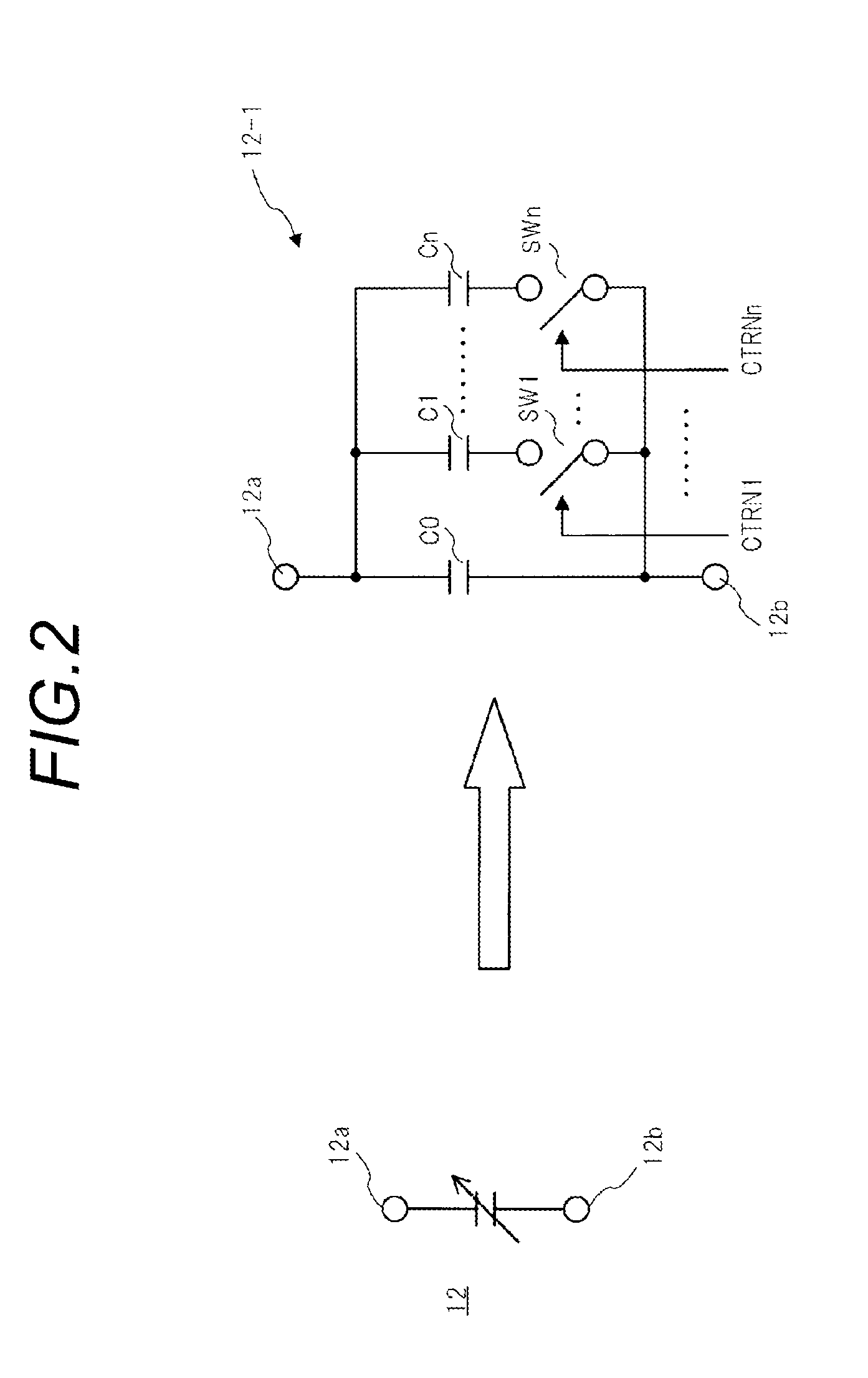
[0086]FIG. 7 is a diagram illustrating an internal configuration of a variable matching circuit 1A according to a modification example of the first embodiment. In the variable matching circuit 1A of this modification example, as the bias circuit 14 for the first transistor circuit in the variable matching circuit 1 illustrated in FIG. 1, a choke coil 16a and a variable voltage source 17a are illustrated, and as the bias circuit 15 for the second transistor circuit, a choke coil 16b and a variable voltage source 17b are illustrated.

[0087]One end of the choke coil 16a is connected to the terminal 11b, the other end thereof is connected to the variable voltage source 17a, and the choke coil 16a transmits a DC potential by being open in terms of AC.

[0088]One end of the choke coil 16b is connected to the terminal 11d, the other end thereof is connected to the variable voltage source 17b, and the choke coil 16b transmits the DC potential by being open in terms of AC.

[0089]The variable vol...

second embodiment

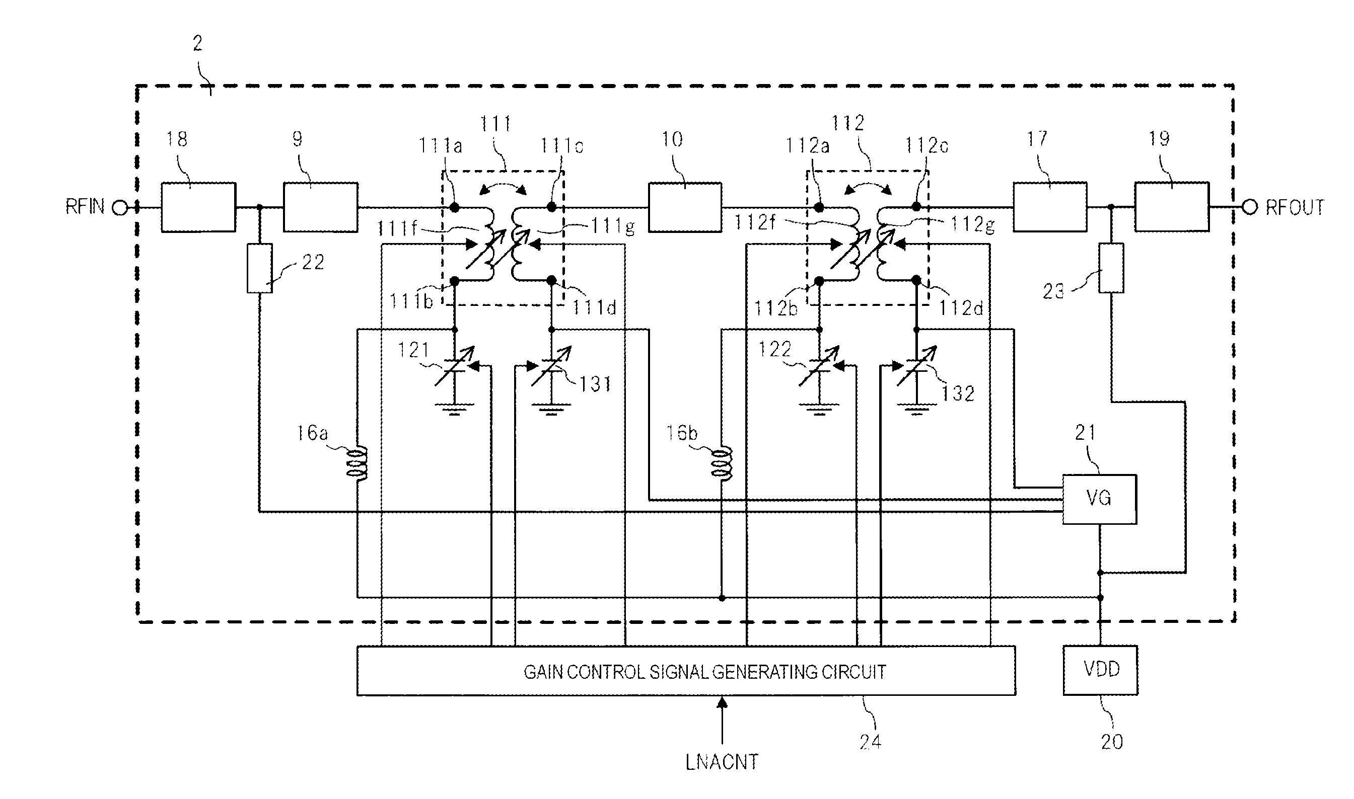
[0097]In the second embodiment, a circuit configuration of the amplifier using the variable matching circuit 1 according to the first embodiment will be described. Furthermore, the same configurations as those of the variable matching circuit 1 according to the first embodiment are represented by the same reference numerals or signs, the description thereof will be omitted or simplified, and different configurations will be described. FIG. 9 is a diagram illustrating a circuit configuration of an amplifier 2 according to the second embodiment. The amplifier 2 is used, for example, as a low noise amplifier (LNA) connected to a following stage of a receiving antenna.

[0098]The amplifier 2 illustrated in FIG. 9 includes an input matching circuit 18, a DC potential transmission circuit 22, two variable matching circuits 1 (refer to FIG. 1), an output matching circuit 19, a DC potential transmission circuit 23, and a DC control voltage generating circuit 21. Among the two variable matchin...


PUM


Abstract

A variable matching circuit includes a transformer which is disposed between first and second transistor circuits. A primary inductor device and a secondary inductor device are magnetically coupled in the transformer. The primary inductor device is connected between an output terminal of the first transistor circuit and a bias circuit for the first transistor circuit. The secondary inductor device is connected between an input terminal of the second transistor circuit and a bias circuit for the second transistor circuit. Connection points between the primary inductor device and the bias circuit for the first transistor circuit and between the secondary inductor device and the bias circuit for the second transistor circuit are connected to first and second capacitive elements, respectively. At least one of inductance values of the respective primary and secondary inductor devices and capacitance values of the respective first and second capacitive elements is variable.

Description

TECHNICAL FIELD[0001]The present disclosure relates to a variable matching circuit and an amplifier which change a gain for amplifying a high frequency signal.BACKGROUND ART[0002]In a Radio-Frequency Integrated Circuit (IC) for inputting and outputting a high frequency signal, a variable gain amplifier for changing a gain is disposed in order to obtain a high frequency signal of electric power in a desired range. When the amplifier is provided with a gain variable function, a performance (for example frequency characteristics, noise figure characteristics, and gain linearity) of the amplifier itself may be degraded.[0003]For example, in a receiver, a low noise amplifier (LNA) for amplifying a signal received by a receiving antenna is usually disposed in a following stage of the receiving antenna. For example, when the low noise amplifier has the variable gain function, performance degradation of the low noise amplifier remarkably appears, resulting in performance degradation of the ...

Claims


Application Information

Patent Timeline
IPC IPC(8): H03G3/00H03F3/00H03F3/193
CPCH03G3/008H03F3/193H03F3/005H03F2200/222H03F2200/451H03F2200/294H03F2200/423H03F1/565H03F3/245H03F3/601H03F2200/408H03F2200/534H03F2200/537H03F2200/541H03G3/3052
Inventor KANEMARU, MASAKI
Owner PANASONIC CORP
Why Eureka
Try Eureka