

Systems and methods for fabrication of superconducting integrated circuits
a technology of integrated circuits and fabrication methods, applied in the direction of superconductor devices, instruments, dissimilar materials junction devices, etc., can solve the problems of contaminating semiconductor facilities, gold can contaminate fabrication tools, and the approach may not make use of quantum gates and circuits, so as to prevent excessive heating and prevent excessive heating
- Summary
- Abstract
- Description
- Claims
- Application Information
AI Technical Summary
Benefits of technology
Problems solved by technology
Method used
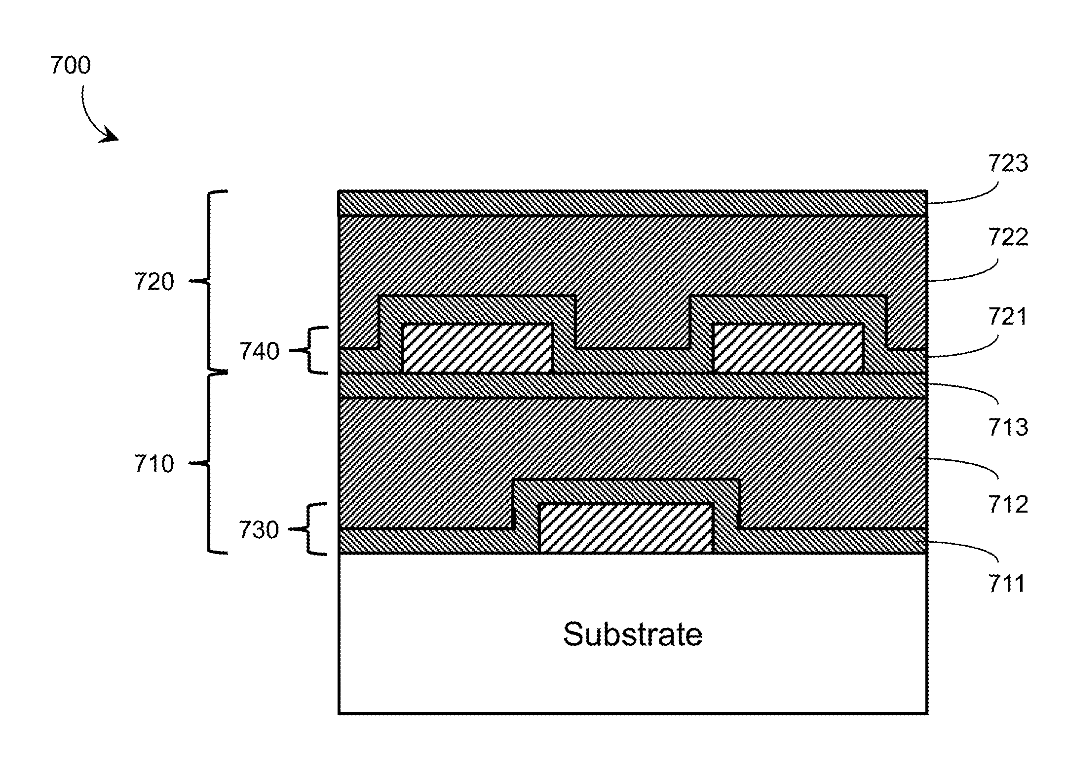
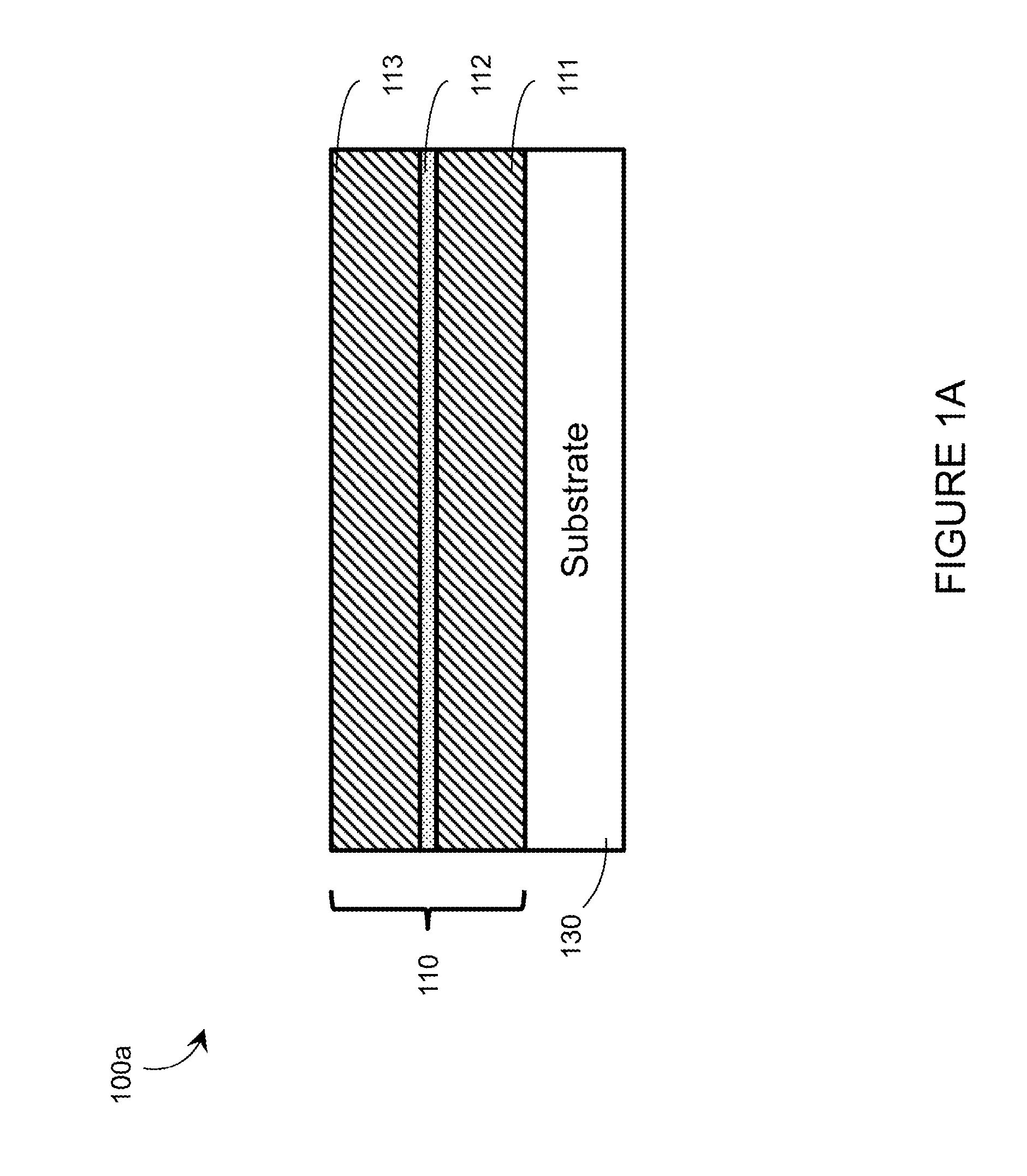
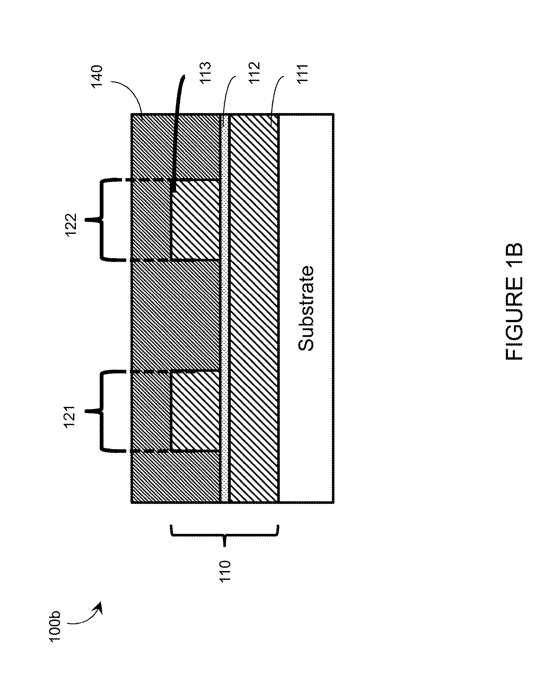
Image

Examples
Embodiment Construction
[0079]In the following description, certain specific details are set forth in order to provide a thorough understanding of various disclosed embodiments. However, one skilled in the relevant art will recognize that embodiments may be practiced without one or more of these specific details, or with other methods, components, materials, etc. In other instances, well-known structures associated with superconductive circuits or structures, quantum computer circuits or structures and / or cryogenic cooling systems such as dilution refrigerators have not been shown or described in detail to avoid unnecessarily obscuring descriptions of the embodiments.
[0080]Unless the context requires otherwise, throughout the specification and claims which follow, the word “comprise” and variations thereof, such as, “comprises” and “comprising” are to be construed in an open, inclusive sense, that is as “including, but not limited to.”
[0081]Reference throughout this specification to “one embodiment” or “an...
PUM
 Abstract
Description
Claims
Application Information