Complementary metal-oxide-semiconductor device

a technology of metal oxides and semiconductors, applied in the field of complementary metal oxidesemiconductor devices, can solve the problems of increasing the vulnerability of external environment, increasing the risk of esd to modern electronics, and often destroying unprotected ics, so as to improve latch-up immunity, increase the holding voltage of the cmos transistor, and increase the layout area

Active Publication Date: 2015-05-07
UNITED MICROELECTRONICS CORP
View PDF6 Cites 19 Cited by
  • Summary
  • Abstract
  • Description
  • Claims
  • Application Information

AI Technical Summary

Benefits of technology

[0008]According to the CMOS device provided by the present invention, a gated diode is provided to separate the pMOS transistor and the nMOS transistor. More important, the gated diode is provided to increase the holding voltage of the CMOS transistor by adding P / N junctions between the pMOS transistor and the nMOS transistor. Briefly speaking, the CMOS device provided by the present invention improves latch-up immunity without increasing layout area.

Problems solved by technology

As products based on ICs become more and more delicate, they also become more and more vulnerable to the impacts from external environment.
For example, it is found that ESD is a constant threat to modern electronics.
The result of ESD on unprotected ICs is often destruction, characterized by melting or explosion of a part of the ICs.
However, conventional ESD protection circuits may be prone to latch-up.
Latch-up is the creation of an undesirable current path between rails, such as VDD and ground, which causes large amounts of current to be drawn from the power supply.
Latch-up may cause circuit malfunction and / or irreversible damage to the ICs.
Therefore, a semiconductor device, particularly the ESD protection semiconductor device, with a simple guard ring and high holding voltage for providing sufficient latch-up avoidance resulting in smaller and more densely packed chip devices is still in need.

Method used


Image

  • Complementary metal-oxide-semiconductor device
  • Complementary metal-oxide-semiconductor device
  • Complementary metal-oxide-semiconductor device

Examples


Embodiment Construction

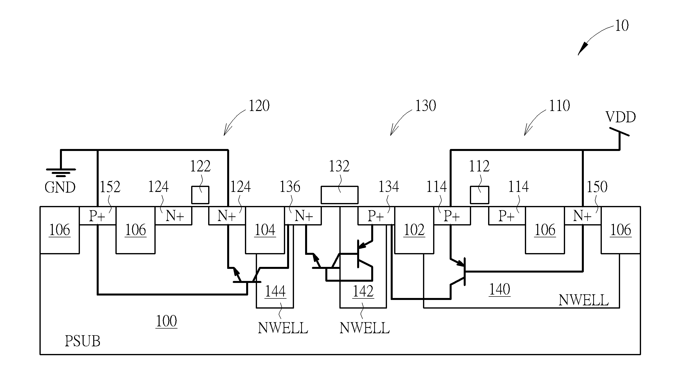
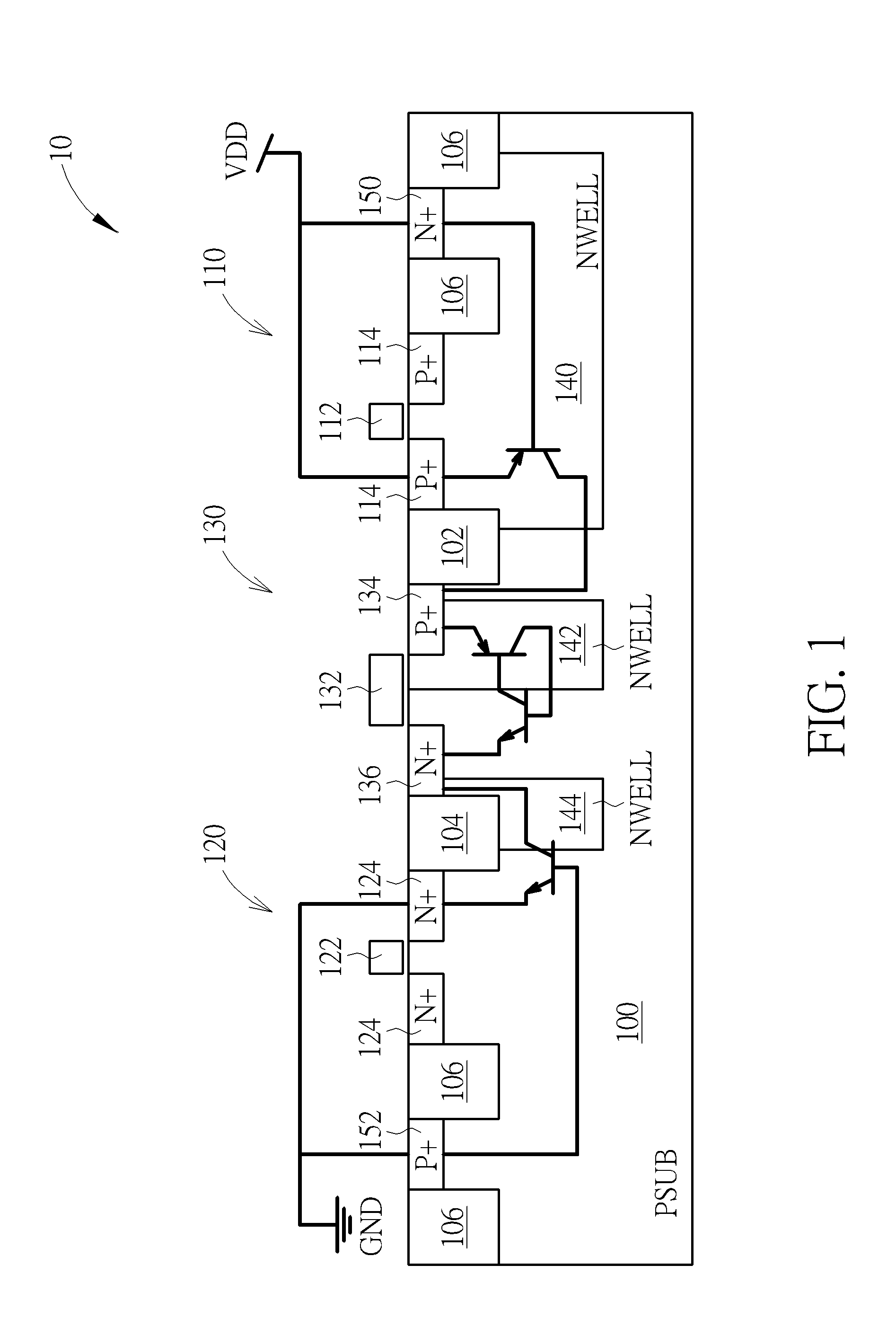
[0020]Please refer to FIG. 1, which is a schematic drawing illustrating a cross-sectional view of a CMOS device provided by a first preferred embodiment of the present invention. According to the first preferred embodiment, a CMOS device 10 is provided. The CMOS device 10 includes a p-typed substrate 100, therefore it can be taken as a p-substrate 100 or a PSUB 100. A pMOS transistor 110, an nMOS transistor 120, and a gated diode 130 are formed on the substrate 100. As shown in FIG. 1, the pMOS transistor 110 includes a p-gate 112 and a p-source / drain 114, and the nMOS transistor 120 includes an n-gate 122 and an n-source / drain 124. It should be noted that the pMOS transistor 110 and the nMOS transistor 120 further include lightly-doped drains (LDDs) of their own conductivity type. And a spacer is respectively formed on sidewalls of the p-gate 112 and the n-gate 122. Though the LDDs and the spacers are omitted from FIG. 1, those skilled in the art would easily realize the placement ...


PUM


Abstract

A CMOS device includes a substrate, a pMOS transistor and an nMOS transistor formed on the substrate, and a gated diode. The gated diode includes a floating gate formed on the substrate in between the pMOS transistor and the nMOS transistor and a pair of a p-doped region and an n-doped region formed in the substrate and between the pMOS transistor and the nMOS transistor. The n-doped region is formed between the floating gate and the nMOS transistor, and the p-doped region is formed between the floating gate and the pMOS transistor.

Description

BACKGROUND OF THE INVENTION[0001]1. Field of the Invention[0002]The invention relates to a complementary metal-oxide-semiconductor (hereinafter abbreviated as CMOS) device, and more particularly, to an electrostatic discharge (hereinafter abbreviated as ESD) protection CMOS device.[0003]2. Description of the Prior Art[0004]Chips and / or Integrated circuits (ICs) are the most essential hardware foundation of the modern information society. As products based on ICs become more and more delicate, they also become more and more vulnerable to the impacts from external environment. For example, it is found that ESD is a constant threat to modern electronics. The result of ESD on unprotected ICs is often destruction, characterized by melting or explosion of a part of the ICs. Therefore, the ESD protection devices are taken as important components of the protection circuitry provided in today' s electronic devices.[0005]However, conventional ESD protection circuits may be prone to latch-up. ...

Claims


Application Information

Patent Timeline
Patent Type & Authority Applications(United States)
IPC IPC(8): H01L27/092H01L27/06H01L23/60H01L29/78
CPCH01L27/0925H01L23/60H01L27/0629H01L29/785H01L27/0274H01L21/823892H01L27/092H01L27/0924
Inventor WANG, CHANG-TZUCHEN, YU-CHUNTANG, TIEN-HAOSU, KUAN-CHENG
Owner UNITED MICROELECTRONICS CORP
Why Eureka
Try Eureka