

Thin film transistor, method of manufacturing same, and image display apparatus
- Summary
- Abstract
- Description
- Claims
- Application Information
AI Technical Summary
Benefits of technology
Problems solved by technology
Method used
Image

Examples
first embodiment
Configuration
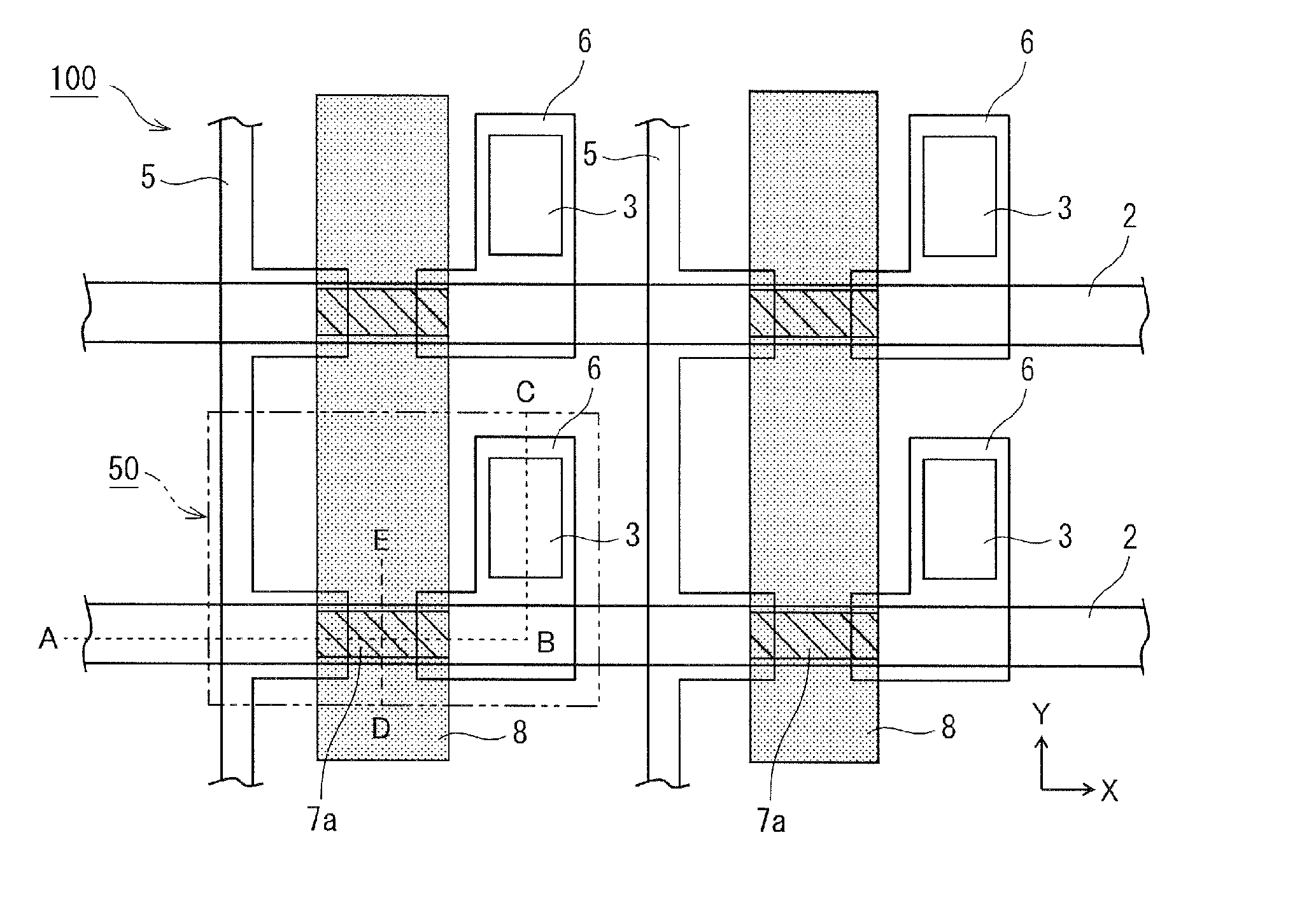
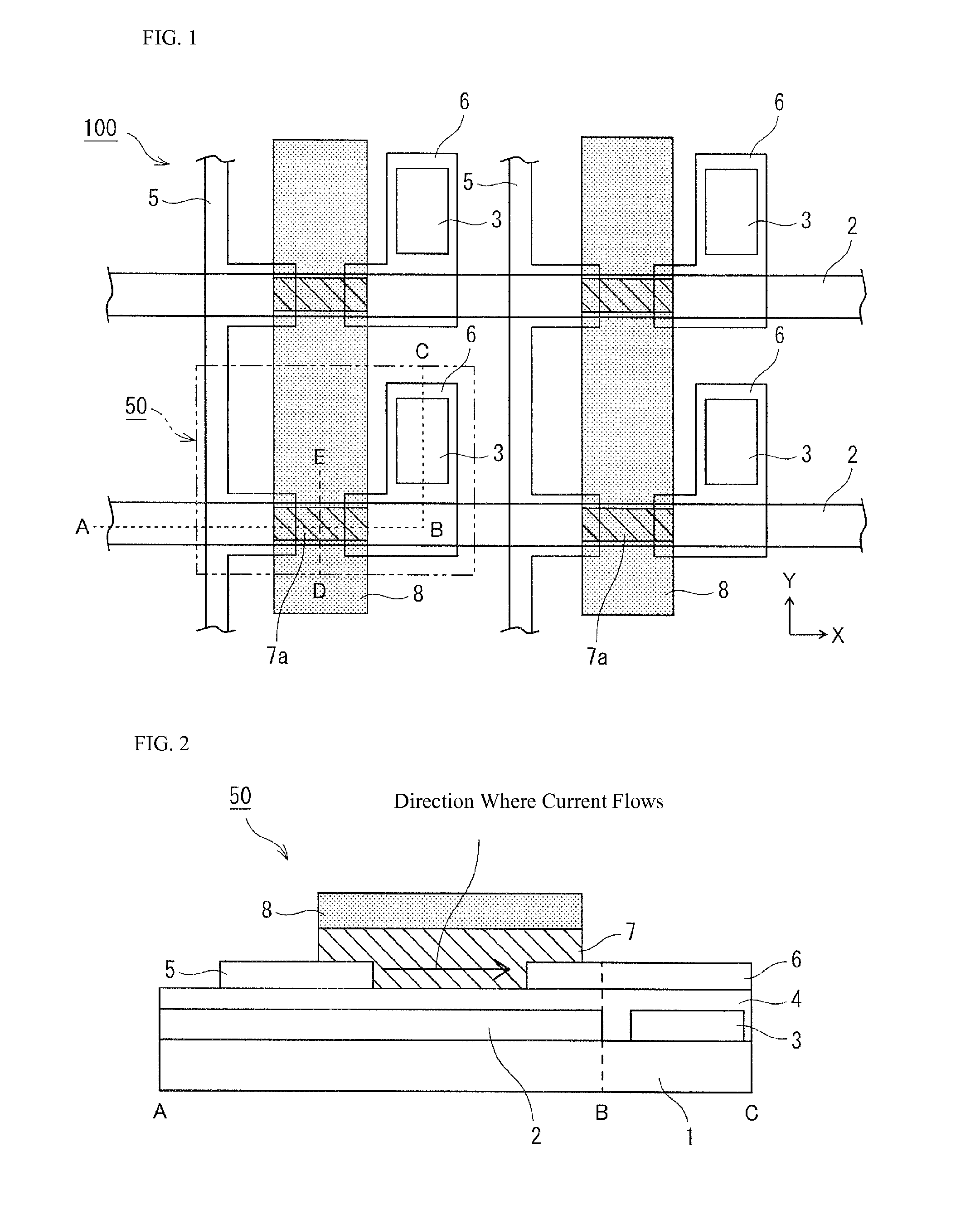
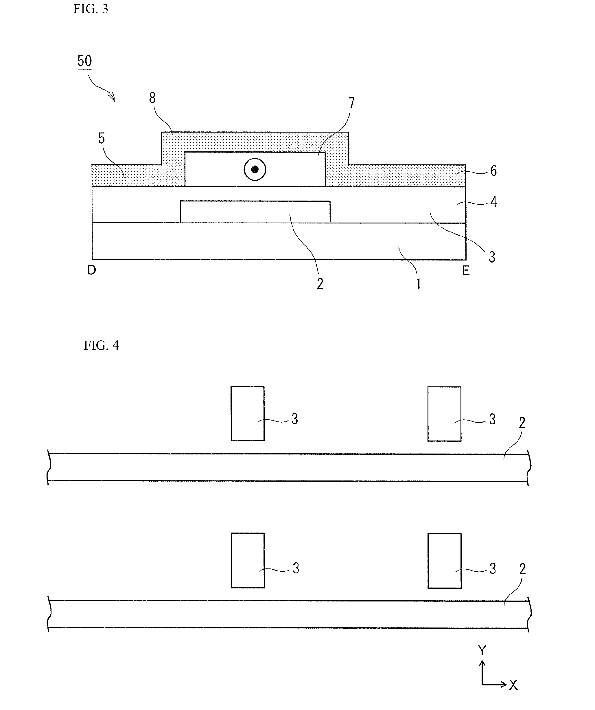
[0052]FIG. 1 is a planar view (perspective view) showing a configuration example of the thin film transistor 100 according to the first embodiment of the present invention. FIG. 2 is a cross-sectional view in which a portion 50 corresponding to one pixel (hereinafter referred to transistor element) is cut along a line A-B-C in the thin film transistor 100 as shown in FIG. 1. FIG. 3 is a cross-sectional view in which the transistor element 50 is cut along a line D-E. In FIG. 1, to avoid complicating the drawing, an illustration of the gate insulation layer 4 is omitted. In FIG. 2, the cross-section A-B and the cross section B-C which is orthogonal to the cross-section A-B are illustrated schematically as a subsequent single cross-section. Moreover, in FIG. 3, a symbol in which a black circle is disposed in a white circle schematically illustrates a current that flows from the reverse side of the paper to the right side of the paper.
[0053]As shown in FIG. 1, the thin film...
second embodiment
Configuration
[0089]FIG. 9 is a planar view (perspective view) showing a configuration example of the thin-film transistor 300 according to a second embodiment of the present invention. FIG. 10 is a cross-sectional view in which a portion 250 corresponding to, for example, one pixel in the thin film transistor 300 as shown in FIG. 9 (hereinafter referred to as a transistor element) is cut along a line A-B-C. FIG. 11 is a cross-sectional view showing the transistor 250 cut along a line D-E. In FIG. 9, to reduce drawing complexity, an illustration of the gate insulation layer 204 is omitted. Further, in FIG. 10, the A-B section and the B-C section which is orthogonal to the A-B section are illustrated schematically in a continuous section. Also, in FIG. 11, a symbol in which a black circle is disposed in a white circle schematically illustrates a current that flows from the reverse side of the paper to the right side of the paper.
[0090]As shown in FIG. 9, the thin film transistor 300 a...
example 1
[0126]The inventor of the present invention produced a thin film transistor array having isolated elements by forming the semiconductor layer 7 in a substantially stripe shape with a coating method as shown in FIG. 6 and the protection layer 8 in a substantially stripe shape which is orthogonal to the semiconductor layer 7 as shown in FIG. 7 and, removing a portion in the semiconductor layer 7 which is exposed from under the protection layer 8 (i.e., a portion not covered by the protection layer 8) (Example 1).
[0127]A manufacturing method of bottom gate / bottom contact type thin film transistor in Example 1 will now be described. First, as a material of the substrate 1, polyethylene naphthalate (PEN) with thickness 125 μm (product of Teijin Dupont) was employed.
[0128]Next, as a material for the gate electrode 2 and the capacitive electrode 3, nanosilver (product of Sumitomo Electric Industries) and nanosilver ink (product of Aldrich) in which weight ratio with respect to polyethylene...
PUM
 Abstract
Description
Claims
Application Information