Array substrate and method for manufacturing the same, and display device

a technology of array substrate and substrate, applied in non-linear optics, instruments, optics, etc., can solve the problems of poor picture quality, flickering, mura, etc., and achieve the effect of eliminating the problem of poor picture quality and poor picture quality

Active Publication Date: 2015-05-14
BOE TECH GRP CO LTD +1
View PDF1 Cites 16 Cited by
  • Summary
  • Abstract
  • Description
  • Claims
  • Application Information

AI Technical Summary

Benefits of technology

[0036]In an embodiment of the invention, in the case that dislocation occurs between the first metal layer and the second metal layer of the array substrate, the area of the overlapping region between the source electrode and the gate electrode of a pixel unit keeps constant, thus the variation on the area of the overlapping region between the source electrode and the gate electrode of each pixel unit is the same as each other (the variation is 0), so that it can be guaranteed to a certain extent that the gray scale of adjacent pixels is uniform and the problem of poor picture quality is eliminated or alleviated.
[0037]In comparison with the prior art, by employing the technical solution of the embodiments of the invention, in the case that dislocation occurs between the first metal layer and the second metal layer, the area of the overlapping region between the gate electrode and the source electrode of adjacent pixel units can also be the same even if the amount of dislocation between the first metal layer and the second metal layer of adjacent pixel units is different, so that the parasitic capacitance Cgs of adjacent pixel units is the same. Therefore, it may be guaranteed that the amount of voltage jump on the pixel electrodes of adjacent pixel units is the same and the gray scale of adjacent pixels is uniform, thereby the problem of poor picture quality, such as Flicker and Mura, etc., may be eliminated or alleviated to a certain extent.

Problems solved by technology

If the amount of voltage jump on the pixel electrodes of adjacent pixel units is different when the parasitic capacitance Cgs of adjacent pixel units is different, the gray scale of the adjacent pixels will be nonuniform, so that poor picture quality will be caused, for example, Flicker (picture flicker) and Mura (nonuniform picture gray scale), etc., will occur.
In conclusion, there exists a problem of poor picture quality when the amount of dislocation between the first metal layer and the second metal layer of adjacent pixel units is different in an existing TFT-LCD.

Method used


Image

  • Array substrate and method for manufacturing the same, and display device
  • Array substrate and method for manufacturing the same, and display device
  • Array substrate and method for manufacturing the same, and display device

Examples


embodiment 1

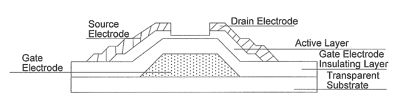
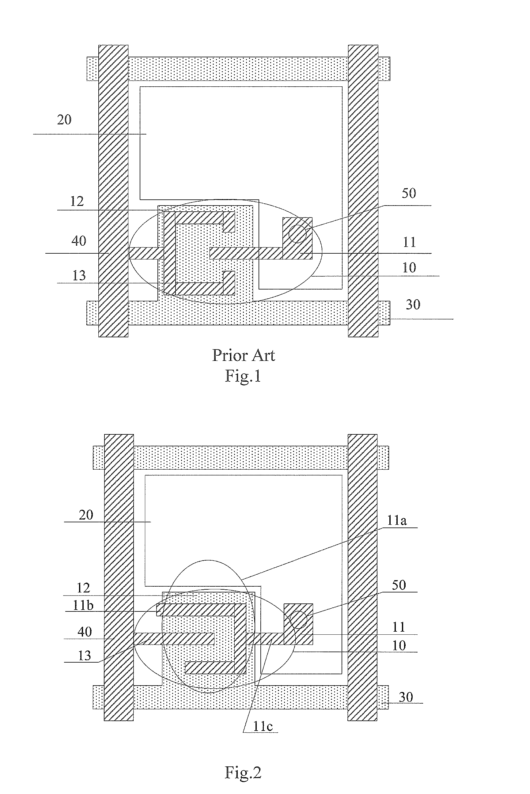
[0075]Preferably, as shown in FIG. 2, the pixel unit includes a TFT 10, a pixel electrode 20, a gate line 30 and a data line 40. The TFT 10 includes a source electrode 11, a gate electrode 12 and a drain electrode 13, wherein the source electrode 11 and the pixel electrode 20 are electrically coupled by a via hole 50, the gate electrode 12 is coupled with the gate line 30, and the drain electrode 13 is coupled with the data line 40. Wherein, the gate electrode 12 and the gate line 30 are located on the first metal layer, and the source electrode 11, the drain electrode 13 and the data line 40 are located on second metal layer.

[0076]The source electrode 11 (or, a lateral section pattern of the source electrode 11) includes an overlapping region 11a with the gate electrode 12 (or, a lateral section pattern of the gate electrode 12, and a first part region 11b and a second part region 11c located respectively on the two sides of the gate electrode 12 (or, a lateral section pattern of t...

embodiment 2

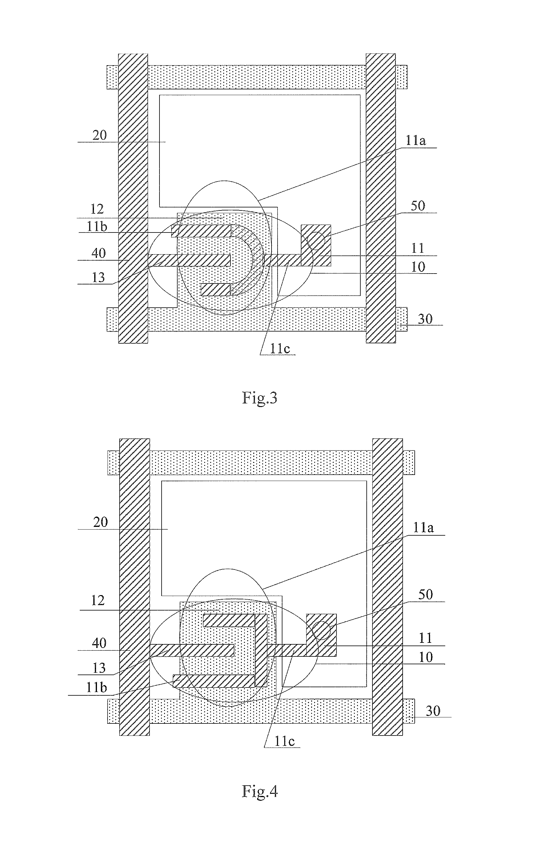
[0097]Preferably, as shown in FIG. 6, the pattern consisted of the first part region 11b, the second part region 11c and the overlapping region 11a with the gate electrode 12 (or, a lateral section pattern of the gate electrode 12) is an analogous ±-shaped pattern. In order to achieve that in the case that dislocation occurs between the first metal layer and the second metal layer, the area of the overlapping region between the source electrode and the gate electrode keeps constant, there exist a plurality of implementing modes for the first part region and the second part region.

[0098]Preferably, the first part region is located at a position on the first side and / or the second side of the ±-shaped pattern that extends out of the gate electrode (or, a lateral section pattern of the gate electrode) in a first direction parallel to the gate line; and the second part region is located at a position on the first side and / or the second side of the ±-shaped pattern that extends out of th...


PUM

PropertyMeasurementUnit
distanceaaaaaaaaaa
widthaaaaaaaaaa
distanceaaaaaaaaaa

Abstract

The invention relates to an array substrate for a display device and to a method for manufacturing an array substrate comprising a thin-film transistor (“TFT”). An array substrate according to an embodiment of the invention comprises a source electrode, a gate electrode and a drain electrode, wherein the gate electrode is located on a first metal layer, the source electrode and the drain electrode are located on a second metal layer, and in the case that dislocation occurs between the first metal layer and the second metal layer, the area of the overlapping region between the source electrode and the gate electrode keeps constant.

Description

CROSS REFERENCE TO RELATED APPLICATION[0001]This application is the U.S. national phase of PCT Application No. PCT / CN2013 / 089974 filed on Dec. 19, 2013, which claims priority to Chinese Patent Application No. 201310311215.0 filed on Jul. 23, 2013, the disclosures of which are incorporated in their entirety by reference herein.FIELD OF THE INVENTION[0002]The present invention relates to the field of display technologies, and in particular, to an array substrate and a method for manufacturing the same, and a display device.DESCRIPTION OF THE PRIOR ART[0003]A Thin-Film Transistor Liquid Crystal Display (TFT-LCD) includes a color film substrate, an array substrate and a liquid crystal layer located between the color film substrate and the array substrate. The array substrate includes: a transparent substrate; and a plurality of gate lines that are parallel to each other and a plurality of electrically insulating data lines that cross the gate lines vertically, which are located on the i...

Claims


Application Information

Patent Timeline
Patent Type & Authority Applications(United States)
IPC IPC(8): H01L27/12H01L29/786H01L29/423H01L29/66
CPCH01L27/124H01L29/66742H01L27/1259H01L29/42384H01L29/786G02F1/1362G02F1/1368H01L29/41733
Inventor JIANG, QINGHUALI, XIAOHELIU, YONGSHAO, XIANJIELI, HONGMIN
Owner BOE TECH GRP CO LTD
Why Eureka
Try Eureka