Optical device and detection device

a detection device and optical technology, applied in the field of optical devices and detection devices, can solve the problems that excessive improvement cannot be expected, and achieve the effect of improving the detection sensitivity of the target molecul

Inactive Publication Date: 2015-05-21
SEIKO EPSON CORP
View PDF6 Cites 9 Cited by
  • Summary
  • Abstract
  • Description
  • Claims
  • Application Information

AI Technical Summary

Benefits of technology

[0012]Some aspects of the invention have an object of providing an optical device and a detection device capable of improving the sensitivity by forming an organic molecular film on a dielectric body between the metal nanostructures, and forming metal nanostructures easy for the target molecules to enter with the distance between the metal nanostructures narrowed.
[0021]The target molecule adsorbed at a position where the distance from the surface of the metal nanostructure becomes the shortest is the target molecule adsorbed on the organic molecular film in the vicinity of the position where the metal nanostructure has contact with the dielectric body. Since the enhanced electric field at that position can be increased, the signal sensitivity can further be enhanced.
[0023]By making the height of the plurality of metal nanostructures from the surface of the dielectric body smaller than the diameter of the metal nanostructure, the target molecule captured between the metal nanostructures having a wide entrance becomes easy to be adsorbed on the organic molecular film formed on the dielectric body between the metal nanostructures with relatively low height.
[0036]The detection device can improve the detection sensitivity of the target molecule.

Problems solved by technology

If the distance between the metal nanostructures is as large as described above, sufficient improvement in excessiveness cannot be expected.

Method used


Image

  • Optical device and detection device
  • Optical device and detection device
  • Optical device and detection device

Examples


first embodiment

1. First Embodiment

1.1. Structure of Optical Device

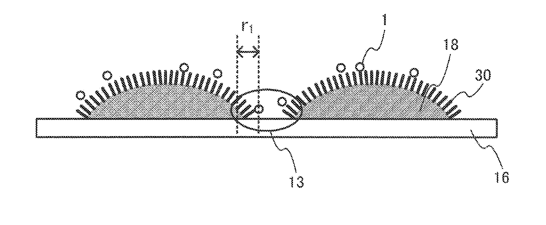
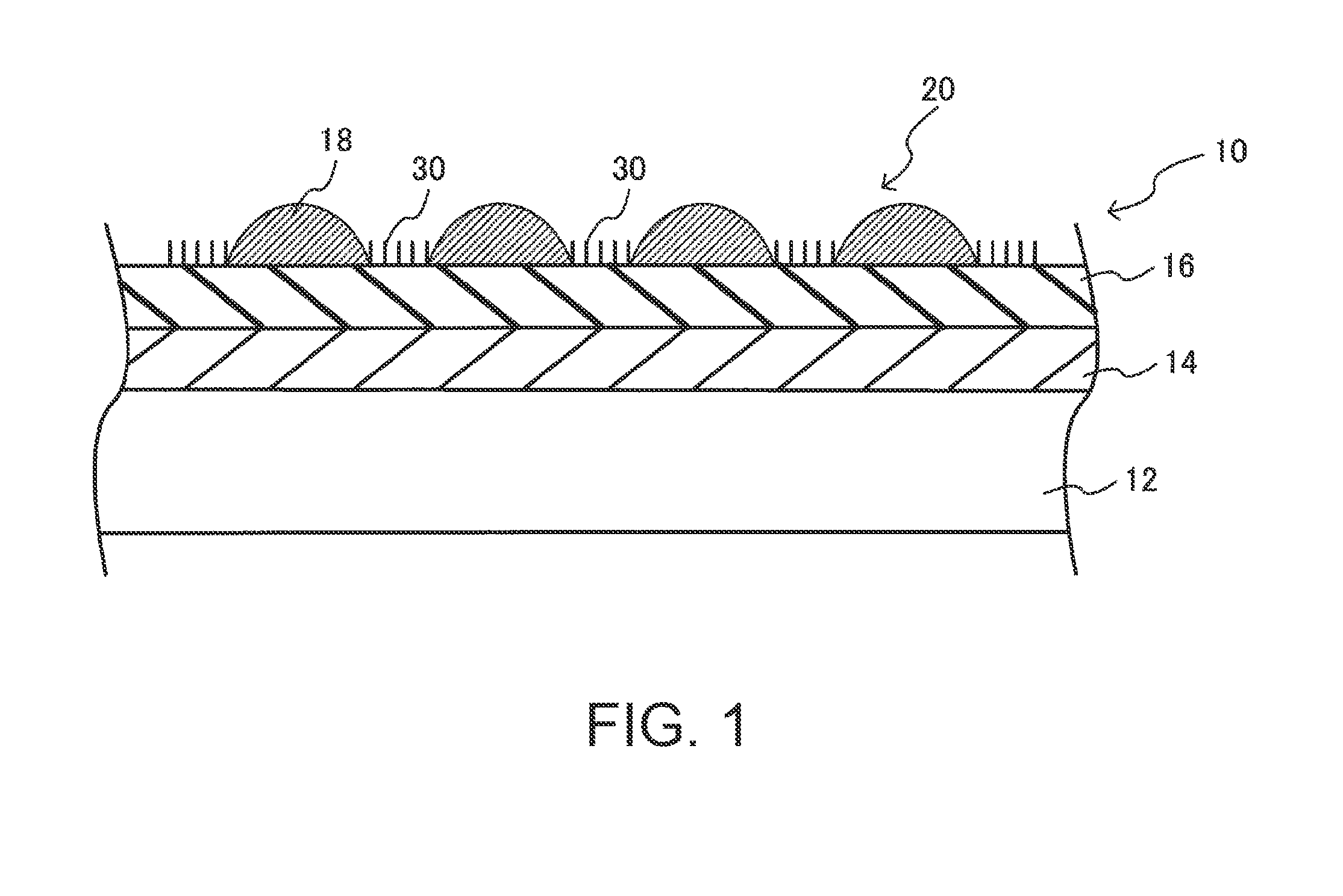
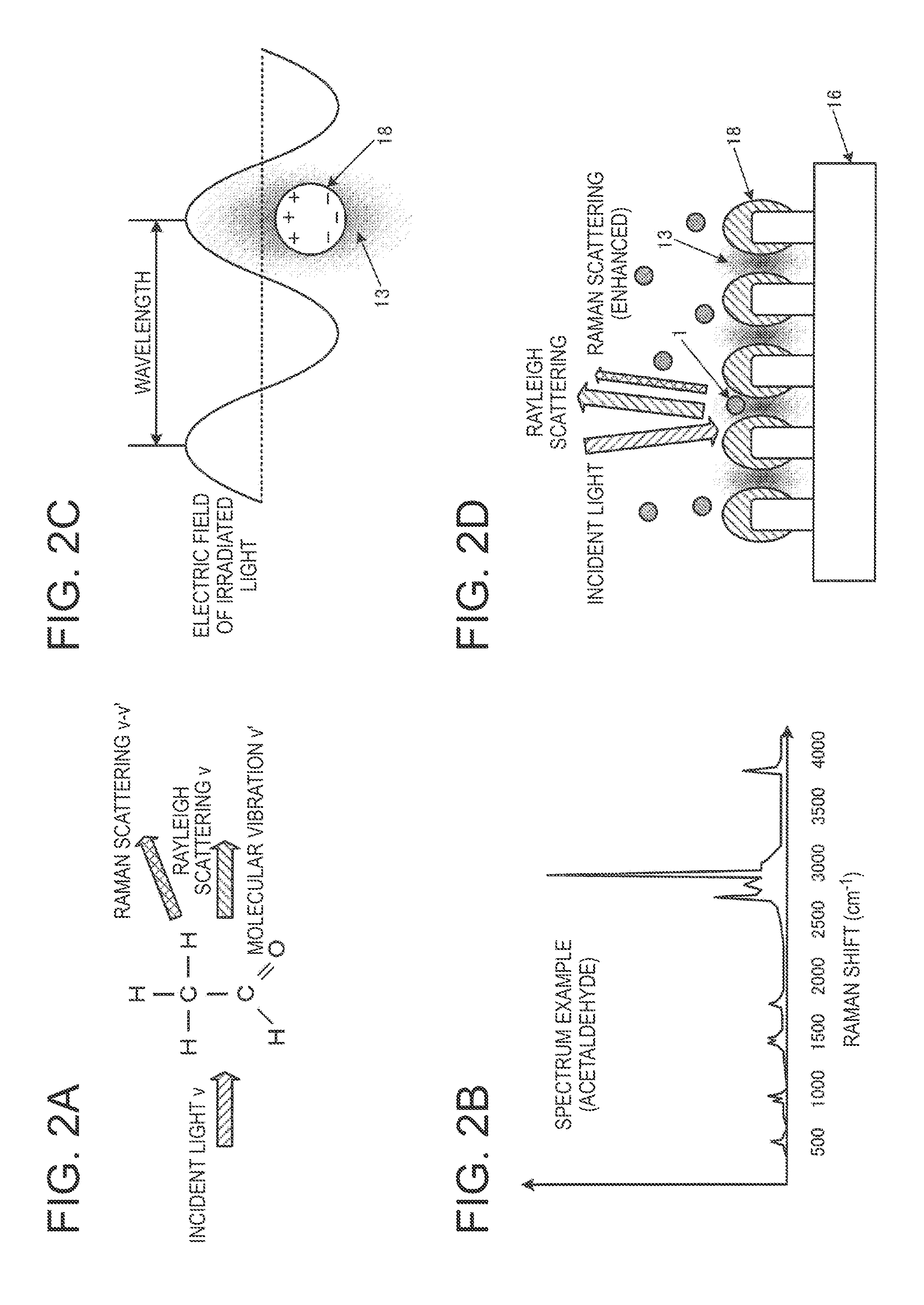
[0061]The optical device 10 shown in FIG. 1 has a dielectric body 16 on the outermost surface of a substrate 12. It is also possible that the substrate 12 itself is a dielectric body such as an oxide, and in such a case, the substrate 12 can be formed of glass, mica, SiO2, SnO2, GeO2, ZrO2, TiO2, Al2O3, PZT, and so on. It is also possible to form the dielectric body 16 described above on the substrate 12 made of a material other than the dielectric body. In the present embodiment, a metal (conductor) film 14 can be provided between, for example, the glass substrate 12 and the dielectric body 16.

[0062]On the dielectric body 16, there are formed metal fine structure 20 formed of a plurality of metal nanostructures 18. The plurality of metal nanostructures 18 can be arranged with a period P. The period P is not limited to a constant value, but a random arrangement with the smallest period P is also possible. The metal nanostructures 18...

second embodiment

2. Second Embodiment

2.1. Overall Configuration of Detection Device

[0096]Then, an overall configuration of the detection device will be explained as a second embodiment. FIG. 18 shows a specific configuration example of the detection device according to the present embodiment. A detection device 100 shown in FIG. 18 has a sample supply channel 101 having a suction port 101A and a dust filter 101B, a sample discharge channel 102 having a discharge port 102A, and an optical device unit 110 provided with an optical device (a sensor chip) 103 having the structure shown in FIG. 4, and so on. Light enters the optical device 103. A housing 120 of the detection device 100 is provided with a sensor cover 122 which can be opened and closed due to a hinge section 121. The optical device unit 110 is disposed inside the sensor cover 122 so as to be detached from the housing 120. The mounted / unmounted state of the optical device unit 110 can be detected by a sensor detector 123.

[0097]The sample su...


PUM

PropertyMeasurementUnit
diameteraaaaaaaaaa
diameteraaaaaaaaaa
diameteraaaaaaaaaa

Abstract

The optical device has a substrate having a dielectric body on a surface, a metal fine structure formed of a plurality of metal nanostructures formed on the dielectric body, and an organic molecular film formed on the dielectric body between the plurality of metal nanostructures, and adapted to capture target molecule. The plurality of metal nanostructures each has a diameter in a planar view of 1 through 500 nm, and has a distance between the metal nanostructures adjacent to each other of no smaller than 0.1 nm and smaller than 10 nm. The plurality of metal nanostructures has the distance between the metal nanostructures adjacent to each other at a second height position H2 from the surface of the dielectric body larger than a first distance between the metal nanostructures adjacent to each other at a first height position H1 (H2>H1) from the surface of the dielectric body.

Description

BACKGROUND[0001]1. Technical Field[0002]The present invention relates to an optical device, a detection device, and so on.[0003]2. Background Art[0004]In recent years, demand for sensor chips used for, for example, medical diagnostics or inspections of food and drink has increased, and further, development of sensor chips high in sensitivity and small in size has been demanded. In order to meet such a demand, a variety of types of sensor chips such as a sensor chip using an electrochemical process have been studied. Among these, sensor chips using a spectroscopic analysis using a surface plasmon resonance (SPR: Surface Plasmon Resonance), in particular, surface enhanced Raman scattering (SERS: Surface Enhanced Raman Scattering) have been receiving increasing attention on the ground of possibility of integration, low cost, applicability in all measurement environments, and so on.[0005]Here, the surface plasmon denotes a vibration mode of an electron wave causing coupling with light u...

Claims


Application Information

Patent Timeline
Patent Type & Authority Applications(United States)
IPC IPC(8): G01N21/65
CPCG01N2610/00G01N21/658B01J2219/00612B01J2219/00637B01J2219/00641B82Y15/00B82Y20/00B82Y30/00G01N21/554G01N21/648G02B6/1226
Inventor YAMADA, AKIKOYAMADA, KOHEI
Owner SEIKO EPSON CORP
Why Eureka
Try Eureka