Vertical Type AC-LED Device and Manufacturing Method Thereof

a manufacturing method and ac-led technology, applied in the field of semiconductor/solid-state device manufacturing, semiconductor devices, electrical devices, etc., can solve the problems of saving transformation element cost, achieve high overload performance, save transformation element cost, and good heat dissipation

Active Publication Date: 2015-05-28
QUANZHOU SANAN SEMICON TECH CO LTD
View PDF1 Cites 30 Cited by
  • Summary
  • Abstract
  • Description
  • Claims
  • Application Information

AI Technical Summary

Benefits of technology

[0006]The present invention discloses a vertical AC LED element with a lateral die and fabrication method thereof. This structure is of good heat dissipation and high overload performance like a vertical chip structure, and at the same time, saves transformation element cost like an AC LED structure does.
[0029]This invention has the following advantages: compared with the traditional lateral AC-LED, which forms the AC-LED either by a) electrical connection of fabricated die through leading or b) by electrical connection of DC-LED during encapsulation, the vertical AC LED disclosed by this invention can be realized in the die process with simple process. Moreover, the conductive substrate outperforms the insulating substrate like sapphire in terms of thermal conductivity, which is more suitable to high current drive. In addition, the light emitting surface of the vertical AC LED disclosed in this invention only requires an electrode bonding pad, thus overcoming the electrode shading problem, improving the light-emitting effect and reducing the raw material cost.

Problems solved by technology

This structure is of good heat dissipation and high overload performance like a vertical chip structure, and at the same time, saves transformation element cost like an AC LED structure does.

Method used


Image

  • Vertical Type AC-LED Device and Manufacturing Method Thereof
  • Vertical Type AC-LED Device and Manufacturing Method Thereof
  • Vertical Type AC-LED Device and Manufacturing Method Thereof

Examples


embodiment 1

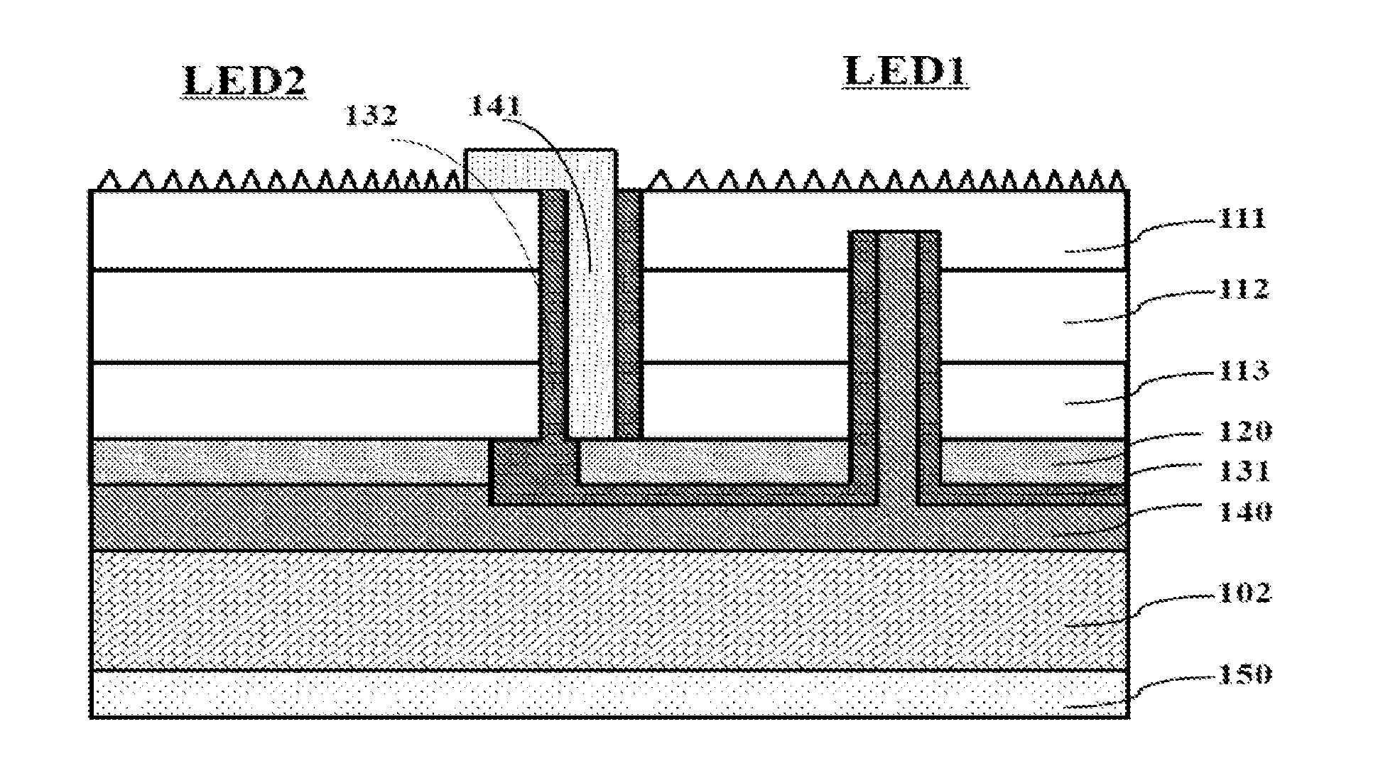
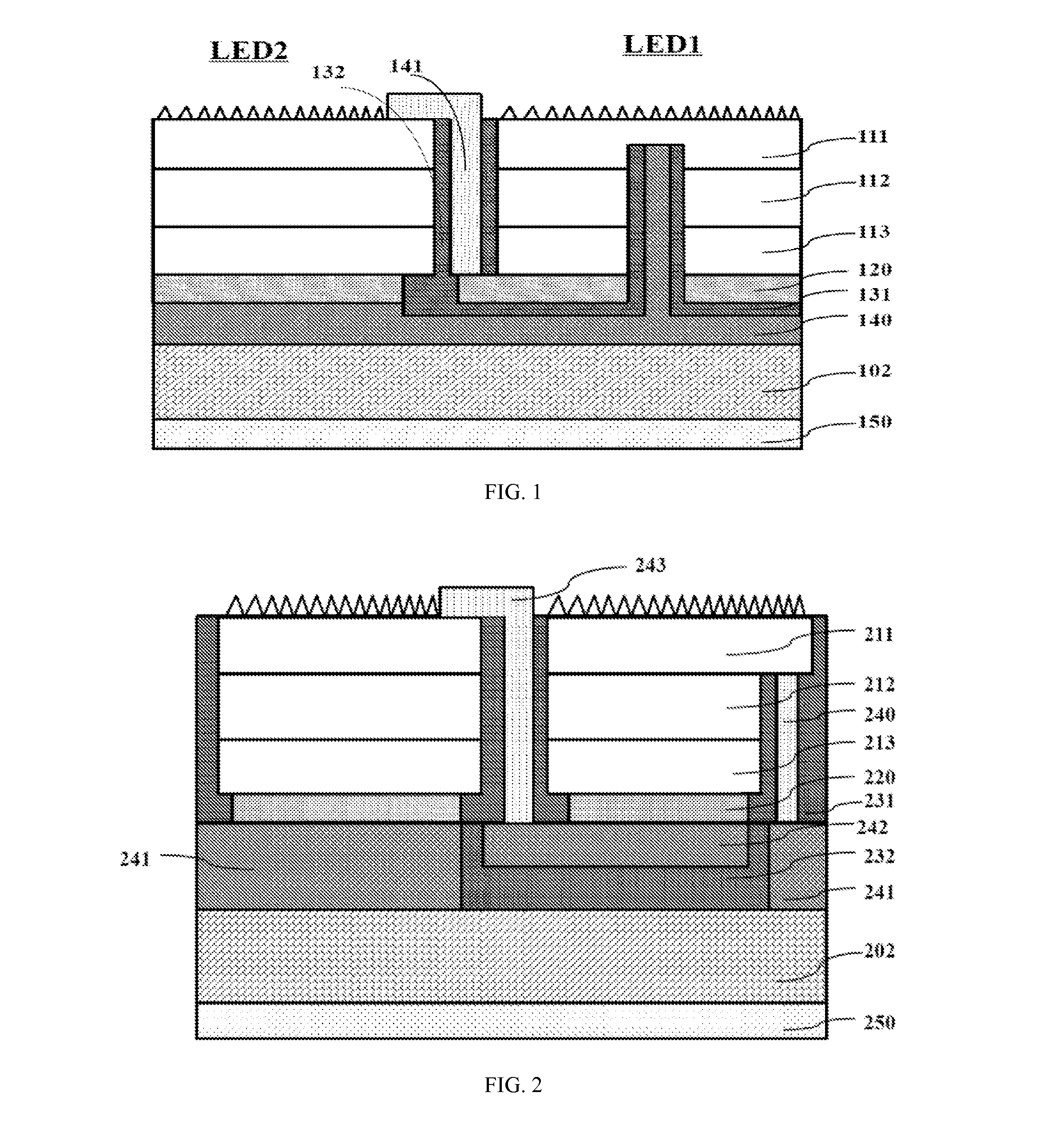
[0039]Referring to FIG. 1, a vertical AC LED element comprises a conductive substrate 102, a light-emitting module, a high reflectivity ohmic contact layer 120, a metal bonding layer 140, a first conductive structure, a second conductive structure and a back electrode 150. The conductive substrate 102, in general, is a material of good heat dissipation. The light-emitting module, comprising an LED 1 and an LED 2, is bonded on the conductive substrate 102 through the metal bonding layer. The LED 1 and LED 2 comprise an n-type semiconductor layer 111, a light-emitting layer 112 and a p-type semiconductor layer 113 from top down, which are mutually isolated from each other, wherein the LED 1 is electrically insulated from the conductive substrate 102 via the insulating layer 131 and the high reflectivity ohmic contact layer 120 is covered on the lower surfaces of the p-type semiconductor layers of LED 1 and LED 2 as well as the part of the isolating region approaching to the LED 1. A c...

embodiment 2

[0053]Referring to FIG. 2, a vertical AC LED element comprises a conductive substrate 202, a light-emitting module, a high reflectivity ohmic contact layer 220, a metal bonding layer 240, insulating layers 231 and 232, a first conductive structure, a second conductive structure and a back electrode 250. The main difference between this embodiment and Embodiment 1 is the position of the insulating layer. In Embodiment 1, the insulating layer is between the metal bonding layer and the p-type semiconductor layer of LED 1. Through the patterned epitaxial layer, the insulating layer is formed on the p-type semiconductor layer of LED 1. However, in this embodiment, the insulating layer is between the metal bonding layer and the conductive substrate. The patterned conductive substrate divides the surface of the insulating layer into two regions, wherein the first region is an insulating region, the surface of which is an insulating material and the second region is a conductive region, the...


PUM


Abstract

The present invention discloses a vertical AC LED element and fabrication method thereof, wherein the vertical AC LED element comprises a conductive substrate (102); a light-emitting module on the conductive substrate (102), including two horizontally arranged in parallel and mutually-isolated LEDs; wherein the first and second LEDs include a first semiconductor layer (111), a light-emitting layer (112) and a second semiconductor layer (113) from top down; a first insulating layer (131) is arranged between the second semiconductor layer (113) of the first LED and the conductive substrate (102) for mutual isolation; an ohmic contact is formed between the second semiconductor layer (113) of the second LED and the conductive substrate (102); a first conductive structure that connects the first semiconductor layer (111) of the first LED, the second semiconductor layer (113) of the second LED and the conductive substrate (102); and a second conductive structure that connects the second semiconductor layer (113) of the first LED and the first semiconductor layer (111) of the second LED.

Description

[0001]This application claims priority to Chinese Patent Application No. 201210157568.5 titled “Vertical AC LED Element and Fabrication Method Thereof”, and filed with the Chinese Patent Office on May 21, 2012, which is hereby incorporated by reference in its entirety.FIELD OF THE INVENTION[0002]The present invention relates to a semiconductor light-emitting element and fabrication method thereof, more particularly, to a vertical alternating current light emitting diode (AC-LED).BACKGROUND OF THE INVENTION[0003]The LED of the solid light-emitting element, owing to such electrical and optical advantages as low energy consumption, long service life, good stability, small size, fast response and stable light-emitting wave length, is widely applied in fields like illumination, household appliance, display and indicator. Moreover, this kind of light-emitting element enjoys considerable progress in light-emitting effect and service life and therefore, is promising to become the mainstream...

Claims


Application Information

Patent Timeline
Patent Type & Authority Applications(United States)
IPC IPC(8): H01L33/08H01L33/62
CPCH01L33/08H01L2933/0066H01L33/62H01L25/0753H01L27/15H01L33/382H01L33/44H01L2924/0002H01L33/0093H01L2924/00
Inventor CHEN, SHUNPINGZENG, XIAOQIANGHUANG, SHAOHUAPAN, QUNFENGWU, JYH-CHIARNG
Owner QUANZHOU SANAN SEMICON TECH CO LTD
Why Eureka
Try Eureka