Method of double-side polishing wafer

a polishing method and wafer technology, applied in the direction of manufacturing tools, lapping machines, abrasive surface conditioning devices, etc., can solve the problems of excessive polishing at the outer circumference of the wafer, easy to occur, and increase the shape of the wafer among polished wafers, so as to achieve stable polishing, high flatness, and maintain stably the effect of the polishing

Active Publication Date: 2015-05-28
SHIN-ETSU HANDOTAI CO LTD
View PDF6 Cites 4 Cited by
  • Summary
  • Abstract
  • Description
  • Claims
  • Application Information

AI Technical Summary

Benefits of technology

[0020]In the present invention, since the direction of revolution of a carrier is reversed every polishing batch while repeating double-side polishing in a batch manner, the carrier can always revolve in a direction opposite a dressing direction of polishing pads, and a dressing condition of the polishing pads

Problems solved by technology

There is a problem in that while a polishing batch is repeated with a double-side polishing apparatus without replacing a polishing pad with a new one, variation in wafer shape among polished wafers gradually increases.
This problem is attributed mainly to the lifetime of th

Method used


Image

  • Method of double-side polishing wafer
  • Method of double-side polishing wafer
  • Method of double-side polishing wafer

Examples


example

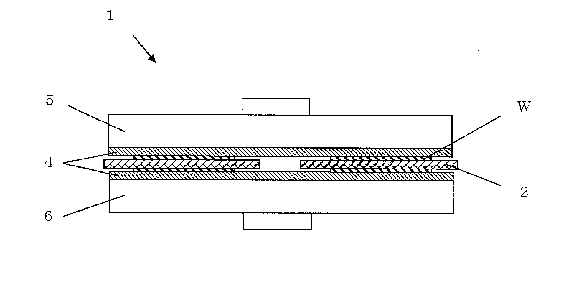
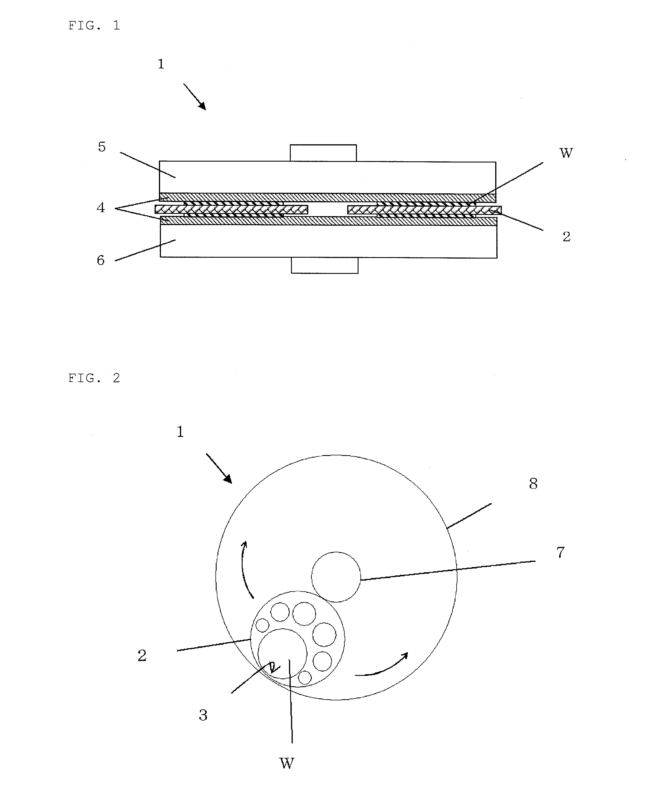
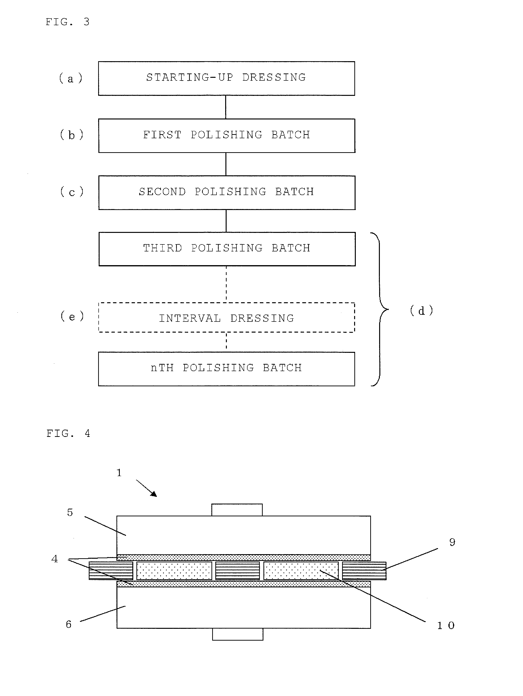
[0055]Five 300-mm-diameter silicon wafers were double-side polished per a single polishing batch with a double-side polishing apparatus (DSP-20B made by Fujikoshi Machinery Corp), as illustrated in FIG. 1, and the polishing batch was repeated until a total of 75 silicon wafers had been double-side polished. The ESFQR (max) of the polished wafers was evaluated with Wafer Sight (made by KLA-Tencor Co., Ltd).

[0056]Used were a titanium carrier including a resin ring formed along the inner circumference of a holding hole, polishing pads (MH S-15A made by nitta haas inc.), and a polishing agent obtained by suspending colloidal silica having a diameter of 35 nm into a KOH-based alkali solution.

[0057]First, starting-up dressing of the polishing pads was performed with a carrier dedicated to dressing and a dressing plate, as illustrated in FIG. 4. The pressing plate used herein was provided with diamond abrasives having a size of #60 on the dressing surfaces. The load was 100 g / cm2 and the d...


PUM

PropertyMeasurementUnit
Surface roughnessaaaaaaaaaa
Sizeaaaaaaaaaa

Abstract

The present invention provides method of double-side polishing a wafer, including: simultaneously polishing both surfaces of the wafer by holding the wafer in a holding hole of a carrier, interposing the held wafer between upper and lower turn tables to which polishing pads are attached, rotating the carrier about an axis of the carrier and revolving the carrier; and repeating the polishing in a batch manner, wherein a direction in which the carrier is revolved is reversed every polishing batch while repeating the polishing in a batch manner. The method enables wafers with high flatness to be stably obtained while inhibiting reduction in productivity due to dressing.

Description

TECHNICAL FIELD[0001]The present invention relates to a double-side polishing method involving interposing a wafer between upper and lower turn tables, to which the respective polishing pads are attached, and simultaneously polishing both surfaces of the wafer.BACKGROUND ART[0002]In manufacture of wafers, such as silicon wafers, conventionally, an ingot is sliced into wafers, the wafers are subjected to, in sequence, lapping, etching, and other processes, and at least a main surface of the wafers is then mirror-polished. This polishing process employs a single-side polishing apparatus for polishing one surface of wafers and a double-side polishing apparatus for simultaneously polishing both surfaces of wafers.[0003]A double-side polishing apparatus includes an upper turn table and a lower turn table, and polishing pads, which are typically made of a nonwoven fabric, are attached to the respective turn tables. FIG. 5 illustrates a four-ways type of a double-side polishing apparatus t...

Claims


Application Information

Patent Timeline
IPC IPC(8): B24B37/08H01L21/304B24B53/017
CPCB24B37/08H01L21/304B24B53/017H01L21/02024
Inventor SATO, KAZUYATANAKA, YUKIKOBAYASHI, SYUICHI
Owner SHIN-ETSU HANDOTAI CO LTD
Why Eureka
Try Eureka