Method for manufacturing semiconductor device

a semiconductor and manufacturing method technology, applied in the direction of semiconductor devices, diodes, radiation controlled devices, etc., can solve the problems of reliability problems, transistor of japanese patent laid-off,

Inactive Publication Date: 2015-06-04
CANON KK
View PDF19 Cites 19 Cited by
  • Summary
  • Abstract
  • Description
  • Claims
  • Application Information

AI Technical Summary

Problems solved by technology

The present inventors, however, found that the transistor of Japanese Patent Laid-Open No. 2008-252032 has a problem with reliability.

Method used


Image

  • Method for manufacturing semiconductor device
  • Method for manufacturing semiconductor device
  • Method for manufacturing semiconductor device

Examples


Embodiment Construction

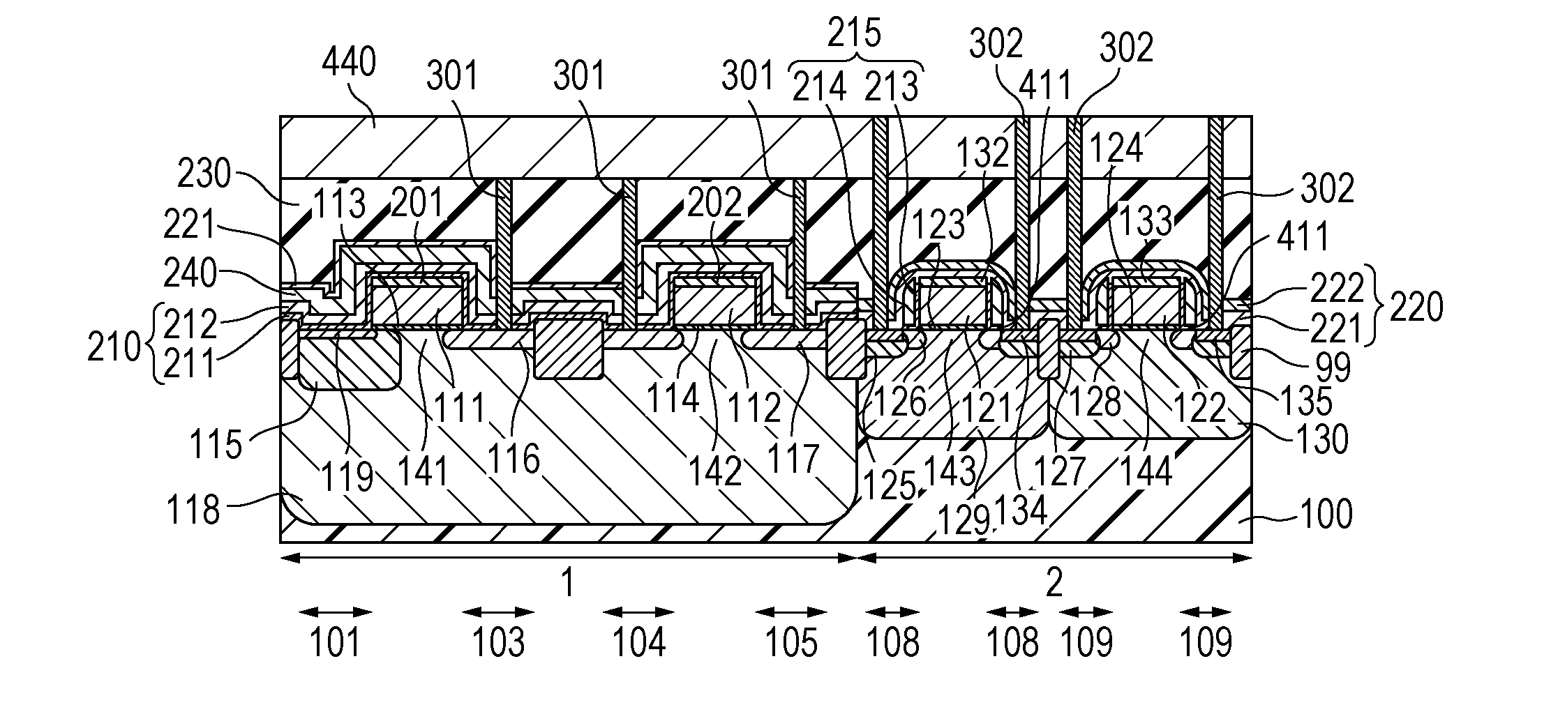
[0014]Embodiments of the invention will now be described with reference to the drawings. In the following description and the drawings, the same reference numerals reference the same parts. The description of the same parts designated by the same reference numerals throughout the drawings may be omitted.

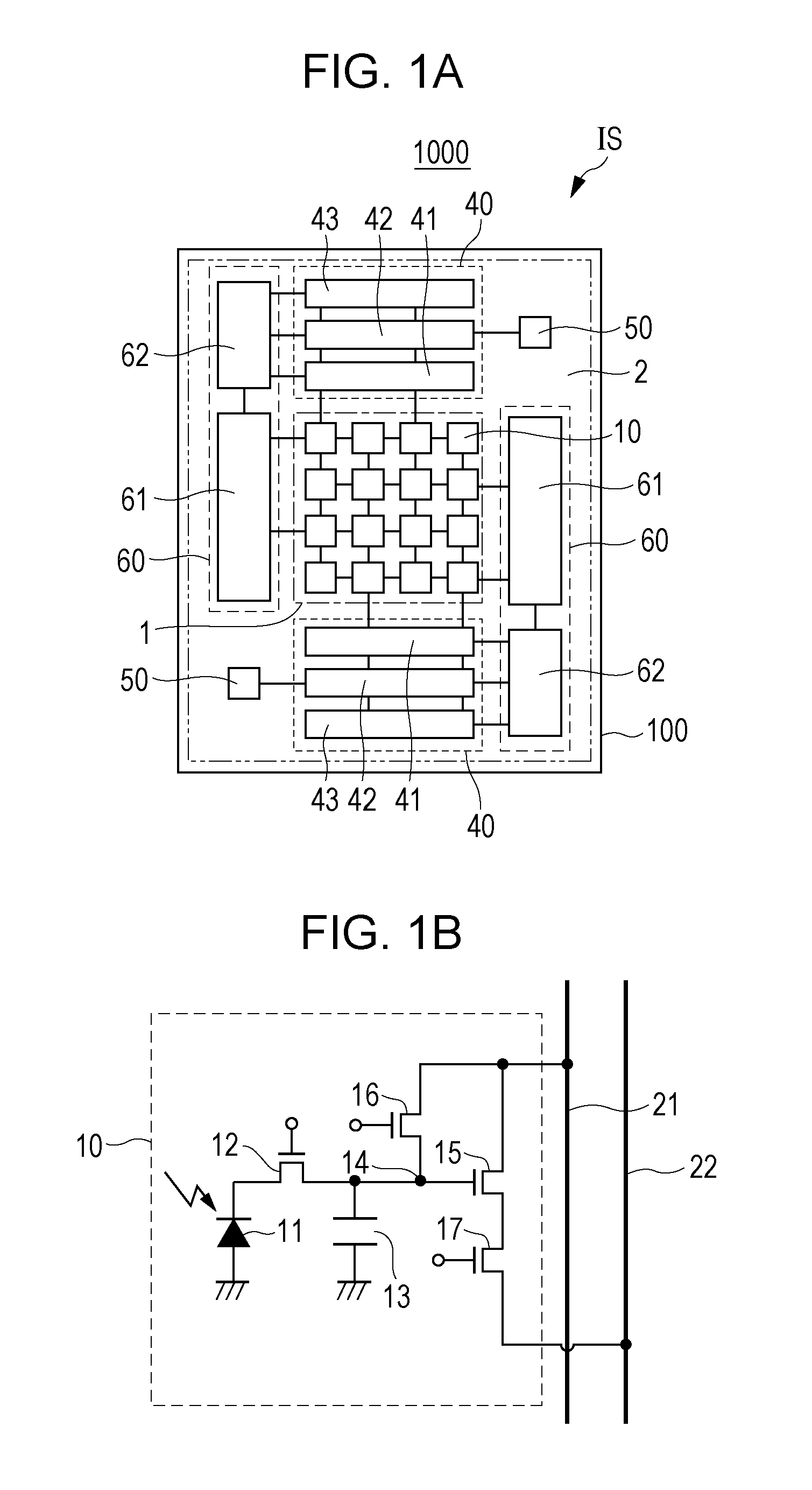
[0015]An image sensing device IS will be described as an embodiment of the semiconductor device of the present application.

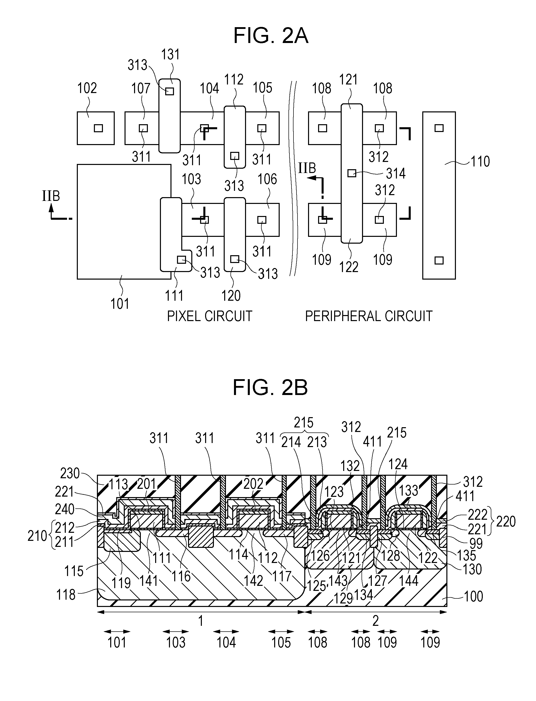
[0016]The semiconductor device 1000 shown in FIG. 1A includes a pixel circuit section 1 in which pixel circuits 10 are arranged 10, and a peripheral circuit section 2 in which peripheral circuits are arranged. The pixel circuit section 1 and the peripheral circuit section 2 are disposed on the same silicon substrate 100. In FIG. 1A, the pixel circuit section 1 is surrounded by a dotted chain line, and the peripheral circuit section 2 is the region between the dotted chain line and a double dotted chain line. The peripheral circuit section 2 lies around the pixel ...


PUM


Abstract

A method includes a step of forming a side wall spacer covering a side surface of a gate electrode of a transistor by etching a first insulator film, and a step of forming a second insulator film covering an upper surface of the gate electrode, the side wall spacer and a source / drain region. The second insulator film is a multilayer film including a silicon oxide layer and a silicon nitride layer. The second step includes forming the silicon oxide layer by thermal CVD so as to come in contact with the side wall spacers, and forming the silicon nitride layer by plasma CVD so as to come in contact with the silicon oxide layer of the second insulator film.

Description

BACKGROUND OF THE INVENTION[0001]1. Field of the Invention[0002]The present application relates to a semiconductor device including an insulated-gate field-effect transistor.[0003]2. Description of the Related Art[0004]Japanese Patent Laid-Open No. 2008-252032 discloses a transistor covered with a silicon nitride film (UV-SiN) formed by plasma CVD using a UV light source and functioning as a hydrogen supplier.SUMMARY OF THE INVENTION[0005]The present inventors, however, found that the transistor of Japanese Patent Laid-Open No. 2008-252032 has a problem with reliability. The reliability refers to that in noise characteristics and long-time reliability of the gate insulating film. Long-time reliability can be estimated by time-dependent dielectric breakdown (TDDB). Negative bias temperature instability (NBTI) may also be an index of long-time reliability.[0006]To solve the problem with reliability, a method is provided for manufacturing a semiconductor device including an insulated-g...

Claims


Application Information

Patent Timeline
Patent Type & Authority Applications(United States)
IPC IPC(8): H01L21/283H01L27/146H01L21/02
CPCH01L21/283H01L21/02164H01L27/14689H01L21/02271H01L21/0217H01L27/14614H01L27/14643H01L21/022H01L21/02274H01L21/28176H01L21/3003H01L29/4983H01L29/518H01L29/665H01L29/6653H01L21/76832
Inventor HIROTA, KATSUNORI
Owner CANON KK
Why Eureka
Try Eureka