Light-emitting element, display module, lighting module, light-emitting device, display device, electronic appliance, and lighting device

a technology of light-emitting elements and display modules, which is applied in the direction of energy-efficient lighting, thermoelectric devices, sustainable buildings, etc., can solve the problems of affecting the practical application of light-emitting elements, and achieve the effects of high emission efficiency, advantageous practical application, and high efficiency

Active Publication Date: 2015-06-04
SEMICON ENERGY LAB CO LTD
View PDF8 Cites 58 Cited by
  • Summary
  • Abstract
  • Description
  • Claims
  • Application Information

AI Technical Summary

Benefits of technology

[0015]The multicolor light-emitting element with the above-described structure has high reliability and is suitable for practical application; on the other hand, a larger number of films need to be formed to obtain one light-emitting element, which hinders the practical application of the light-emitting element.
[0056]In another embodiment of the present invention, a display module, a lighting module, a light-emitting device, a display device, an electronic appliance, and a lighting device that can be fabricated at low cost by using any of the above-described light-emitting elements can be provided.

Problems solved by technology

The multicolor light-emitting element with the above-described structure has high reliability and is suitable for practical application; on the other hand, a larger number of films need to be formed to obtain one light-emitting element, which hinders the practical application of the light-emitting element.

Method used


Image

  • Light-emitting element, display module, lighting module, light-emitting device, display device, electronic appliance, and lighting device
  • Light-emitting element, display module, lighting module, light-emitting device, display device, electronic appliance, and lighting device
  • Light-emitting element, display module, lighting module, light-emitting device, display device, electronic appliance, and lighting device

Examples


example 1

[0247]In this example, methods of fabricating Light-emitting elements 1 to 3 each of which is one embodiment of the present invention and Light-emitting element 4 which is a comparative light-emitting element and characteristics thereof are described. Structural formulae of organic compounds used for Light-emitting elements 1 to 4 are shown below.

(Method of Fabricating Light-Emitting Element 1)

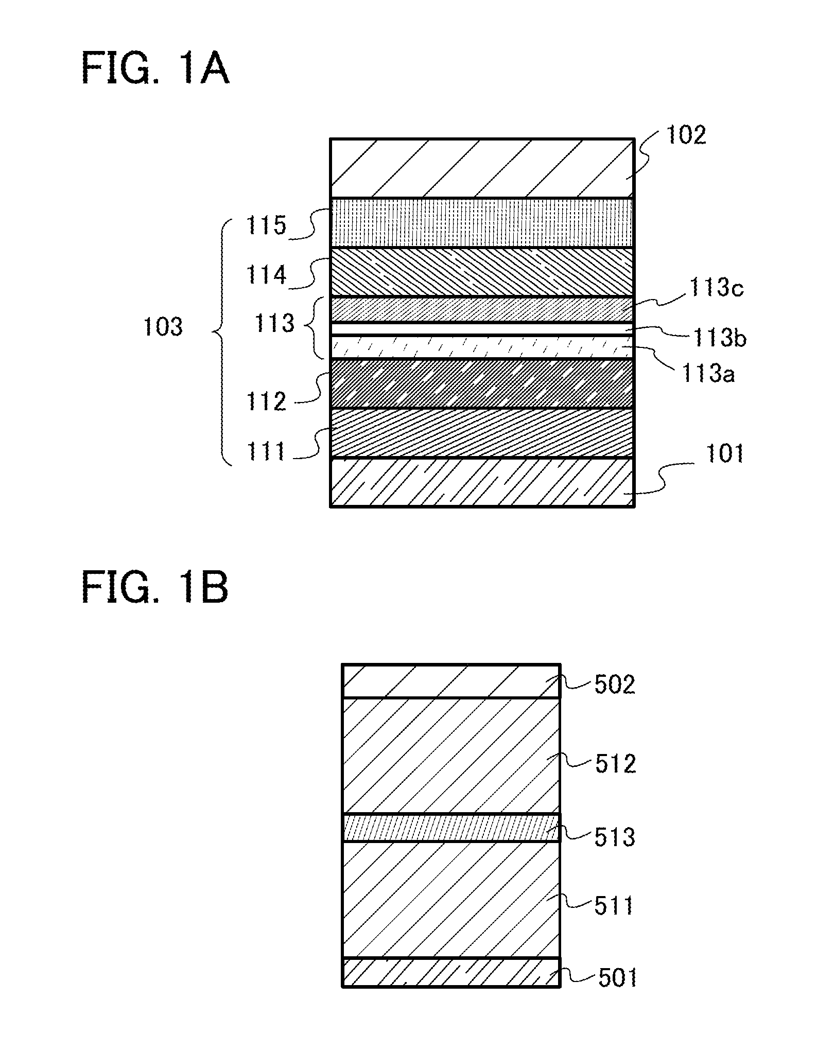
[0248]A film of indium tin oxide containing silicon oxide (ITSO) was formed over a glass substrate by a sputtering method to form the first electrode 101. The thickness was 110 nm and the electrode area was 2 mm×2 mm. Here, the first electrode 101 functions as an anode of the light-emitting element.

[0249]Next, in pretreatment for forming the light-emitting element over the substrate, a surface of the substrate was washed with water and baked at 200° C. for 1 hour, and then UV ozone treatment was performed for 370 seconds.

[0250]After that, the substrate was transferred into a vacuum evaporation...

example 2

[0267]In this example, a method of fabricating Light-emitting element 5 which is one embodiment of the present invention and characteristics thereof are described. Structural formulae of organic compounds used for Light-emitting element 5 are shown below.

(Method of Fabricating Light-Emitting Element 5)

[0268]A film of indium tin oxide containing silicon oxide (ITSO) was formed over a glass substrate by a sputtering method to form the first electrode 101. The thickness was 110 nm and the electrode area was 2 mm×2 mm. Here, the first electrode 101 functions as an anode of the light-emitting element.

[0269]Next, in pretreatment for forming the light-emitting element over the substrate, a surface of the substrate was washed with water and baked at 200° C. for 1 hour, and then UV ozone treatment was performed for 370 seconds.

[0270]After that, the substrate was transferred into a vacuum evaporation apparatus where the pressure had been reduced to approximately 10−4 Pa, and was subjected to ...

example 3

[0286]In this example, methods of fabricating Light-emitting elements 6 and 7 each of which is one embodiment of the present invention and characteristics thereof are described. Structural formulae of organic compounds used for Light-emitting elements 6 and 7 are shown below.

(Method of Fabricating Light-Emitting Element 6)

[0287]A film of indium tin oxide containing silicon oxide (ITSO) was formed over a glass substrate by a sputtering method to form the first electrode 101. The thickness was 110 nm and the electrode area was 2 mm×2 mm. Here, the first electrode 101 functions as an anode of the light-emitting element.

[0288]Next, in pretreatment for forming the light-emitting element over the substrate, a surface of the substrate was washed with water and baked at 200° C. for 1 hour, and then UV ozone treatment was performed for 370 seconds.

[0289]After that, the substrate was transferred into a vacuum evaporation apparatus where the pressure had been reduced to approximately 10−4 Pa, ...


PUM


Abstract

An object of one embodiment of the present invention is to provide a multicolor light-emitting element that utilizes fluorescence and phosphorescence and is advantageous for practical application. The light-emitting element has a stacked-layer structure of a first light-emitting layer containing a host material and a fluorescent substance, a separation layer containing a substance having a hole-transport property and a substance having an electron-transport property, and a second light-emitting layer containing two kinds of organic compounds that form an exciplex and a substance that can convert triplet excitation energy into luminescence. Note that a light-emitting element in which light emitted from the first light-emitting layer has an emission spectrum peak on the shorter wavelength side than an emission spectrum peak of the second light-emitting layer is more effective.

Description

TECHNICAL FIELD[0001]One embodiment of the present invention relates to a light-emitting element containing an organic compound as a light-emitting substance, a display module, a lighting module, a display device, a light-emitting device, an electronic appliance, and a lighting device.[0002]Note that one embodiment of the present invention is not limited to the above technical field. The technical field of one embodiment of the invention disclosed in this specification and the like relates to an object, a method, or a manufacturing method. In addition, one embodiment of the present invention relates to a process, a machine, manufacture, or a composition of matter. Specifically, examples of the technical field of one embodiment of the present invention disclosed in this specification include a semiconductor device, a display device, a liquid crystal display device, a light-emitting device, a lighting device, a power storage device, a storage device, a method of driving any of them, a...

Claims


Application Information

Patent Timeline
Patent Type & Authority Applications(United States)
IPC IPC(8): H01L51/50H01L51/00
CPCH01L51/504H01L51/5016H01L51/0054H01L51/5072H01L51/0052H01L51/5056H10K85/342H10K50/121H10K50/131H10K50/11H10K2101/10H10K2101/27H10K2101/90H10K2101/20Y02B20/00H10K2102/351H10K50/15H10K50/16H10K59/32H10K85/611H10K85/615H10K85/622H10K85/626H10K85/633H10K85/636H10K85/654H10K85/6572H10K85/6576
Inventor OHSAWA, NOBUHARUNONAKA, YUSUKEISHISONE, TAKAHIROSEO, SATOSHIKAWATA, TAKUYA
Owner SEMICON ENERGY LAB CO LTD
Why Eureka
Try Eureka