Substrate treatment method and substrate treatment apparatus

Active Publication Date: 2015-06-11
DAINIPPON SCREEN MTG CO LTD
View PDF8 Cites 17 Cited by
  • Summary
  • Abstract
  • Description
  • Claims
  • Application Information

AI Technical Summary

Benefits of technology

[0005]In a production process for a semiconductor device of MOSFET (Metal Oxide Semiconductor Field Effect Transistor) type, for example, a silicon nitride film is formed as a side wall film on a lateral side of a gate electrode of polysilicon formed on a front surface of a semiconduc

Problems solved by technology

Therefore, the etching step for the removal of the silicon oxide film and the silicon nitride film requires a longer period of time.
When the phosphoric acid aqueous solution and water are mixed together and the resulting phosphoric acid aqueous solution/water mixture is supplied to a nozzle, the phosphoric acid aqueous solution/water mixture is liable to experience a bumping phenomenon due to the mixing to flow through the nozzle in a water vapor containing state.
Thus, the phosphoric acid aqueous solution/water mixture is unstably

Method used


Image

  • Substrate treatment method and substrate treatment apparatus
  • Substrate treatment method and substrate treatment apparatus
  • Substrate treatment method and substrate treatment apparatus

Examples


first embodiment

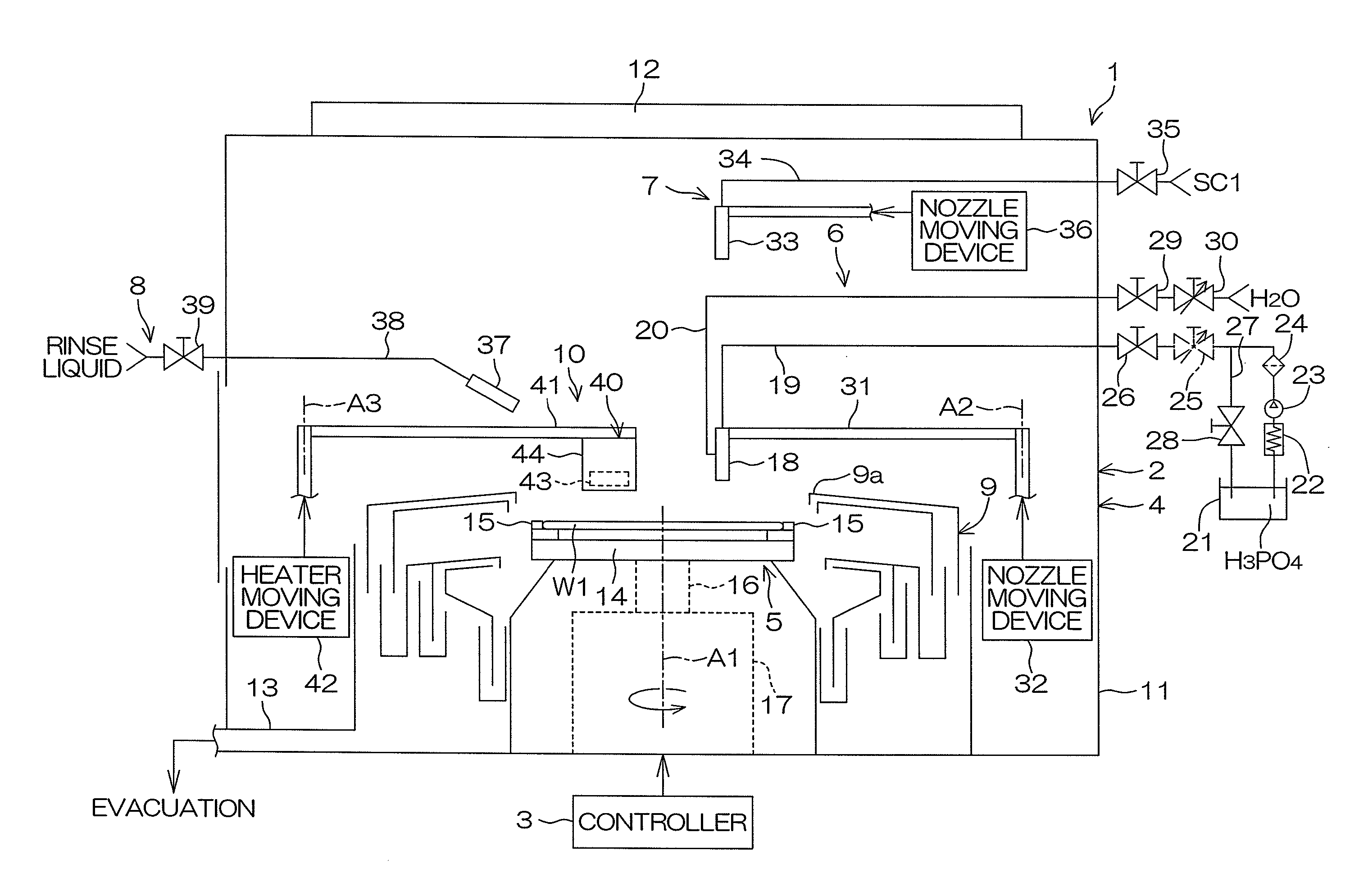
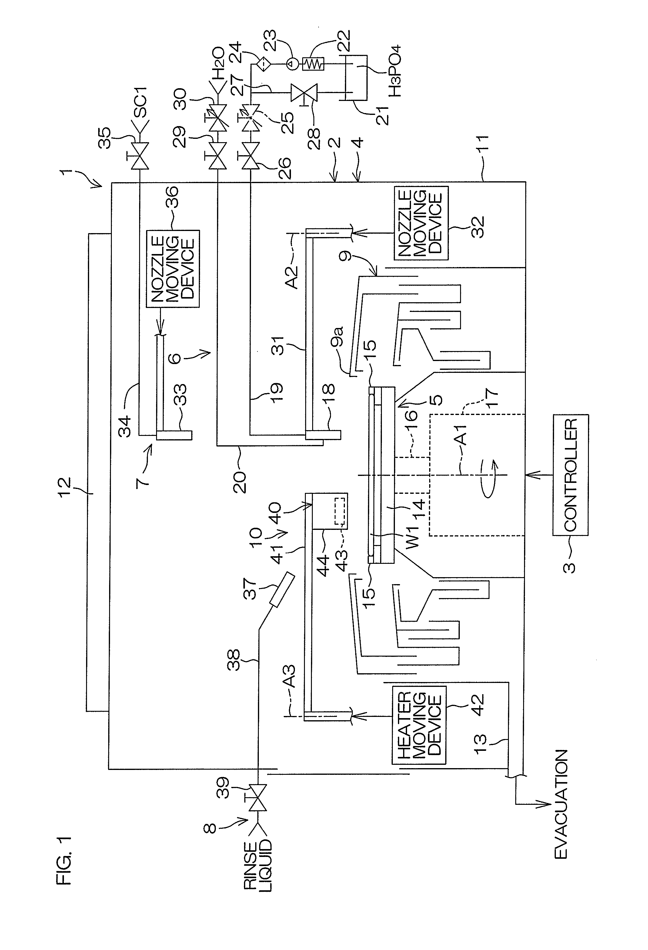
[0078]FIG. 1 is a schematic diagram showing the inside of a treatment unit 2 of a substrate treatment apparatus 1 according to the present invention as seen horizontally.

[0079]The substrate treatment apparatus 1 is of a single substrate treatment type adapted to treat a single substrate W1 at a time. The substrate W1 to be treated by the substrate treatment apparatus 1 is, for example, a round semiconductor wafer (semiconductor substrate). The substrate treatment apparatus 1 includes a plurality of treatment units 2 (only one of which is shown in FIG. 1) each adapted to etch a silicon nitride film (SiN, Si3N4 or the like) and to etch a silicon oxide film (SiO2) by supplying a phosphoric acid aqueous solution (an aqueous solution containing phosphoric acid as a major component) to a front surface (upper surface) of the substrate W1 having a device formation region, and a controller (control unit) 3 which controls the operations of devices provided in the substrate treatment apparatus...

second embodiment

[0168] the controller 3 controls the first and second phosphoric acid valves 117, 127 to switch the phosphoric acid aqueous solution supply source between the first phosphoric acid supplying unit 110 and the second phosphoric acid supplying unit 120 to supply the phosphoric acid aqueous solution from the supply source to the phosphoric acid nozzle 103. Thus, the concentration of the phosphoric acid aqueous solution to be spouted from the phosphoric acid nozzle 103 can be changed with a simplified construction.

[0169]A three-way valve may be provided between the phosphoric acid valve 117 and the first filter 114 in the first phosphoric acid line 107, which is branched into the first return line 115 via the three-way valve. The controller 3 may control the three-way valve so as to selectively feed out the phosphoric acid aqueous solution flowing through the first phosphoric acid line 107 into the phosphoric acid nozzle 103 or into the first return line 115. Further, a three-way valve m...

third embodiment

[0170]FIG. 9 is a schematic diagram showing the inside of a treatment unit 202 of a substrate treatment apparatus 201 according to the present invention as seen horizontally.

[0171]The substrate treatment apparatus 201 is of a single substrate treatment type adapted to treat a single disk-shaped substrate W2 (e.g., semiconductor wafer) at a time. The substrate treatment apparatus 201 includes a plurality of treatment units 202 (only one of which is shown in FIG. 9) each adapted to treat the substrate W2 with a treatment fluid such as a treatment liquid or a treatment gas, and a controller (retention space switching unit) 203 which controls the operations of devices provided in the substrate treatment apparatus 201 and the opening / closing operations of valves. A single treatment unit 202 may be provided in the substrate treatment apparatus 201.

[0172]In the third embodiment, components corresponding to those in the first embodiment are designated by the same reference characters as in ...


PUM

PropertyMeasurementUnit
Timeaaaaaaaaaa
Flow rateaaaaaaaaaa
Concentrationaaaaaaaaaa

Abstract

A substrate treatment method for treating a substrate including a first silicon nitride film provided on a front surface thereof and a silicon oxide film provided on the first silicon nitride film to remove the first silicon nitride film and the silicon oxide film from the substrate includes: a first phosphoric acid treatment step of supplying a phosphoric acid aqueous solution having a predetermined first concentration to the substrate held by a substrate holding unit to treat the substrate with the first concentration phosphoric acid aqueous solution for the removal of the first silicon nitride film; and a second phosphoric acid treatment step of supplying a phosphoric acid aqueous solution having a second concentration lower than the first concentration to the substrate to treat the substrate with the second concentration phosphoric acid aqueous solution for the removal of the silicon oxide film after the first phosphoric acid treatment step.

Description

BACKGROUND OF THE INVENTION[0001]1. Field of the Invention[0002]The present invention relates to a substrate treatment method and a substrate treatment apparatus for treating a substrate with a treatment liquid. Examples of the substrate to be treated include semiconductor wafers, glass substrates for liquid crystal display devices, substrates for plasma display devices, substrates for FED (Field Emission Display) devices, substrates for optical disks, substrates for magnetic disks, substrates for magneto-optical disks, substrates for photo masks, ceramic substrates and substrates for solar cells.[0003]2. Description of Related Art[0004]In production processes for semiconductor devices and the like, a higher temperature phosphoric acid aqueous solution is supplied as an etching liquid to a front surface of a substrate formed with a silicon nitride film, as required, for etching off the silicon nitride film. US Patent Application No. 2012 / 074102 A1 discloses a substrate treatment app...

Claims


Application Information

Patent Timeline
IPC IPC(8): H01L21/67H01L21/311H01L29/66
CPCH01L21/67075H01L21/6708H01L21/31111H01L29/6653H01L21/311H01L21/67028H01L21/67115
Inventor HINODE, TAIKIOTA, TAKASHISAITO, KAZUHIDE
Owner DAINIPPON SCREEN MTG CO LTD
Why Eureka
Try Eureka