Electrostatic protection circuit and semiconductor integrated circuit apparatus

a technology of electrostatic protection circuit and semiconductor integrated circuit, which is applied in the direction of electrical equipment, emergency protective arrangements for limiting excess voltage/current, and semiconductor devices, can solve the problems of unavoidable cost increase, complicated manufacturing process of semiconductor integrated circuit apparatus, and internal circuit destruction, so as to prevent the destruction of internal circuit caused by electrostatic discharge. excellent

Active Publication Date: 2015-06-11
SEIKO EPSON CORP
View PDF13 Cites 23 Cited by
  • Summary
  • Abstract
  • Description
  • Claims
  • Application Information

AI Technical Summary

Benefits of technology

[0024]It is preferable that the discharge circuit includes one of: an N-channel transistor having a drain connected to the first node, a source connected to the second node, and a gate to which the output signal of the detection circuit is supplied; and an NPN transistor having a collector connected to the first node, an emitter connected to the second node, and a base to which the output signal of the detection circuit is supplied. The N-channel transistor or the NPN transisto...

Problems solved by technology

As a result, the N-channel transistor 14 is placed in an off state without sufficient discharge of the accumulated electric charge, which may result in destruction of an internal circuit.
Furthermore, while an N-channel transistor 11b h...

Method used


Image

  • Electrostatic protection circuit and semiconductor integrated circuit apparatus
  • Electrostatic protection circuit and semiconductor integrated circuit apparatus
  • Electrostatic protection circuit and semiconductor integrated circuit apparatus

Examples


first embodiment

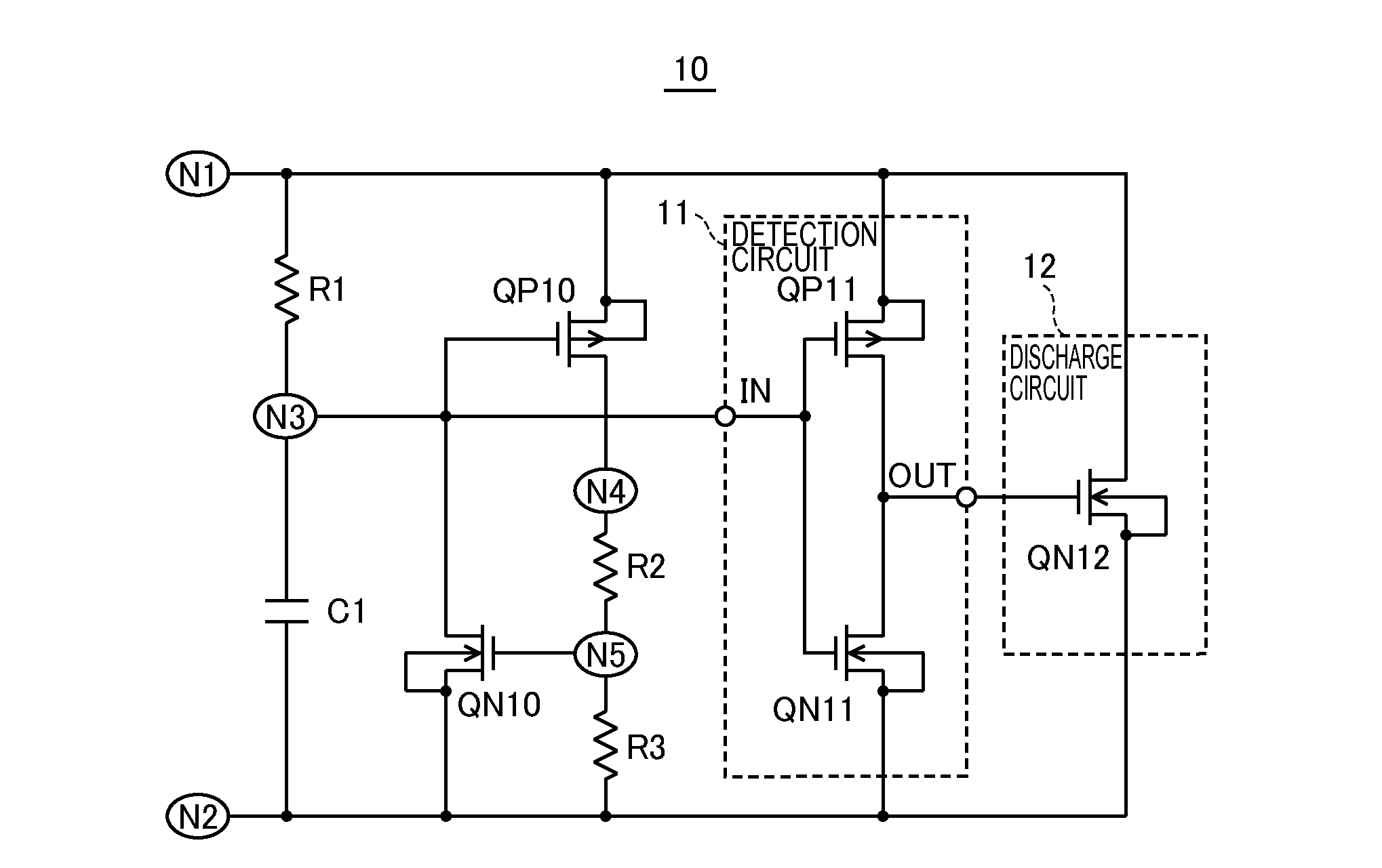
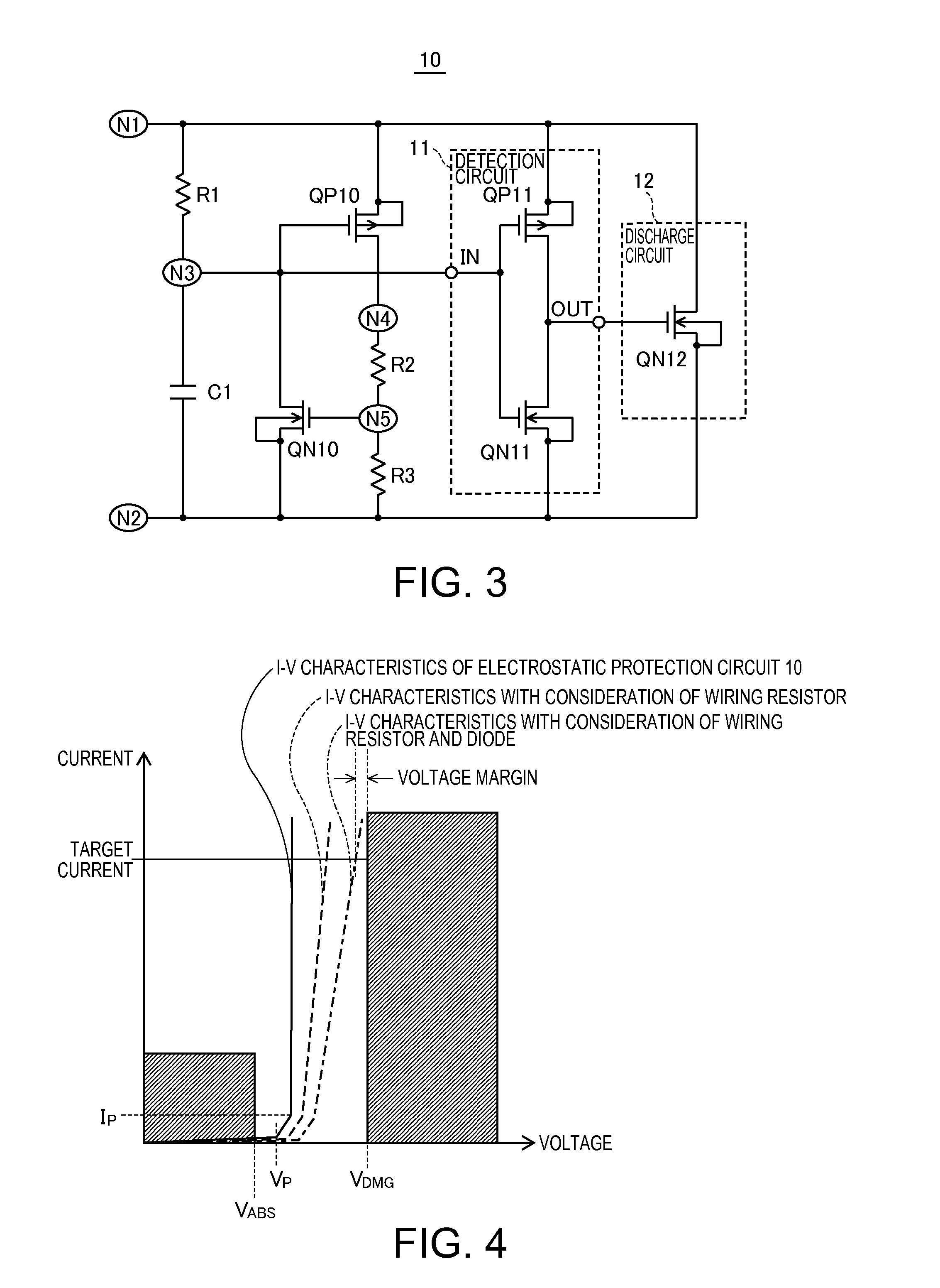
[0052]FIG. 3 is a circuit diagram showing an example of a configuration of an electrostatic protection circuit according to a first embodiment of the invention. As shown in FIG. 3, an electrostatic protection circuit 10 includes resistor elements R1 to R3 as first to third impedance elements, a capacitor C1, a P-channel MOS transistor QP10 as a first transistor, an N-channel MOS transistor QN10 as a second transistor, a detection circuit 11, and a discharge circuit 12.

[0053]The electrostatic protection circuit 10 is connected via a node N1 to a first terminal to which a potential of a high-potential side is supplied, and is connected via a node N2 to a second terminal to which a potential of a low-potential side is supplied. A series circuit including the resistor element R1 and the capacitor C1, which are connected to each other by the node N3, is connected between the node N1 and the node N2. In the present embodiment, the resistor element R1 is connected between the node N1 and t...

second embodiment

[0077]FIG. 6 is a circuit diagram showing an example of a configuration of an electrostatic protection circuit according to a second embodiment of the invention. As compared to the electrostatic protection circuit 10 according to the first embodiment shown in FIG. 3, an electrostatic protection circuit 10a according to the second embodiment additionally includes an N-channel MOS transistor QN13 as a third transistor connected in parallel to a resistor element R2, and may further include a resistor element R4. In other regards, the electrostatic protection circuit 10a shown in FIG. 6 is similar to the electrostatic protection circuit 10 shown in FIG. 3.

[0078]The transistor QN13 has a drain, a source, and a gate that are connected to one end of the resistor element R2, the other end of the resistor element R2, and an output terminal OUT of a detection circuit 11, respectively, and turns on when an output signal of the detection circuit 11 is activated to a high level. The resistor ele...

third embodiment

[0090]FIG. 8 is a circuit diagram showing an example of a configuration of an electrostatic protection circuit according to a third embodiment of the invention. An electrostatic protection circuit 10b according to the third embodiment is realized by connecting a plurality of resistor elements in series between a node N4 and a node N5 in the electrostatic protection circuit 10 according to the first embodiment shown in FIG. 3, and by adding at least one N-channel transistor that is connected in parallel with at least one of these resistor elements. In other regards, the electrostatic protection circuit 10b shown in FIG. 8 is similar to the electrostatic protection circuit 10 shown in FIG. 3.

[0091]FIG. 8 exemplarily shows resistor elements R4 to R6 that are connected in series between the node N4 and the node N5, and N-channel MOS transistors QN14 and QN15 that are connected in parallel to the resistor elements R5 and R6, respectively. In this way, a plurality of transistors may be pr...


PUM


Abstract

The following are included: a series circuit that is connected between a first node and a second node and includes an impedance element and a capacitor connected to each other by a third node; a first transistor that is connected between the first node and a fourth node and turns on in accordance with an increase in voltage generated in the impedance element; a voltage divider circuit that divides voltage between the fourth node and the second node; a second transistor that turns on in accordance with an increase in the divided voltage and increases current flowing in the impedance element; a detection circuit that activates an output signal upon detection of an on state of the second transistor; and a discharge circuit that allows current to flow from the first node to the second node when the output signal of the detection circuit is activated.

Description

BACKGROUND[0001]1. Technical Field[0002]The present invention relates to an electrostatic protection circuit for protecting a semiconductor integrated circuit apparatus from electrostatic discharge (ESD). The invention further relates to a semiconductor integrated circuit apparatus embedded with such an electrostatic protection circuit.[0003]2. Related Art[0004]A semiconductor integrated circuit apparatus may be provided with an electrostatic protection circuit to prevent destruction of an internal circuit caused by static electricity. In general, an electrostatic protection circuit is connected between a first terminal to which a potential of a high-potential side is supplied and a second terminal to which a potential of a low-potential side is supplied. For example, when a positive electric charge is applied to the first terminal due to electrostatic discharge, the positive electric charge is discharged to the second terminal via the electrostatic protection circuit. In this case,...

Claims


Application Information

Patent Timeline
IPC IPC(8): H02H9/04
CPCH02H9/04H02H9/046H01L27/0248
Inventor IKEDA, MASUHIDE
Owner SEIKO EPSON CORP
Why Eureka
Try Eureka