Electrostatic protection circuit and semiconductor integrated circuit apparatus

Active Publication Date: 2015-06-11
SEIKO EPSON CORP
View PDF13 Cites 19 Cited by
  • Summary
  • Abstract
  • Description
  • Claims
  • Application Information

AI Technical Summary

Benefits of technology

[0028]Also, it is preferable that the discharge circuit includes one of: an N-channel transistor having a drain connected to the first node, a source connected to the second node, and a gate to which the output signal of the detection circuit is supplied; and an NPN transistor having a collector connected to the first node, an emitter connected to the second node, and a base to which the output signal of the detection circuit is supplied. The N-channel transistor or the NPN transisto

Problems solved by technology

As a result, the N-channel transistor14 is placed in an off state without sufficient discharge of the accumulated electric charge, which may result in destruction of an internal circuit.
Furthermore, while an N-channel transistor 11b havi

Method used


Image

  • Electrostatic protection circuit and semiconductor integrated circuit apparatus
  • Electrostatic protection circuit and semiconductor integrated circuit apparatus
  • Electrostatic protection circuit and semiconductor integrated circuit apparatus

Examples


first embodiment

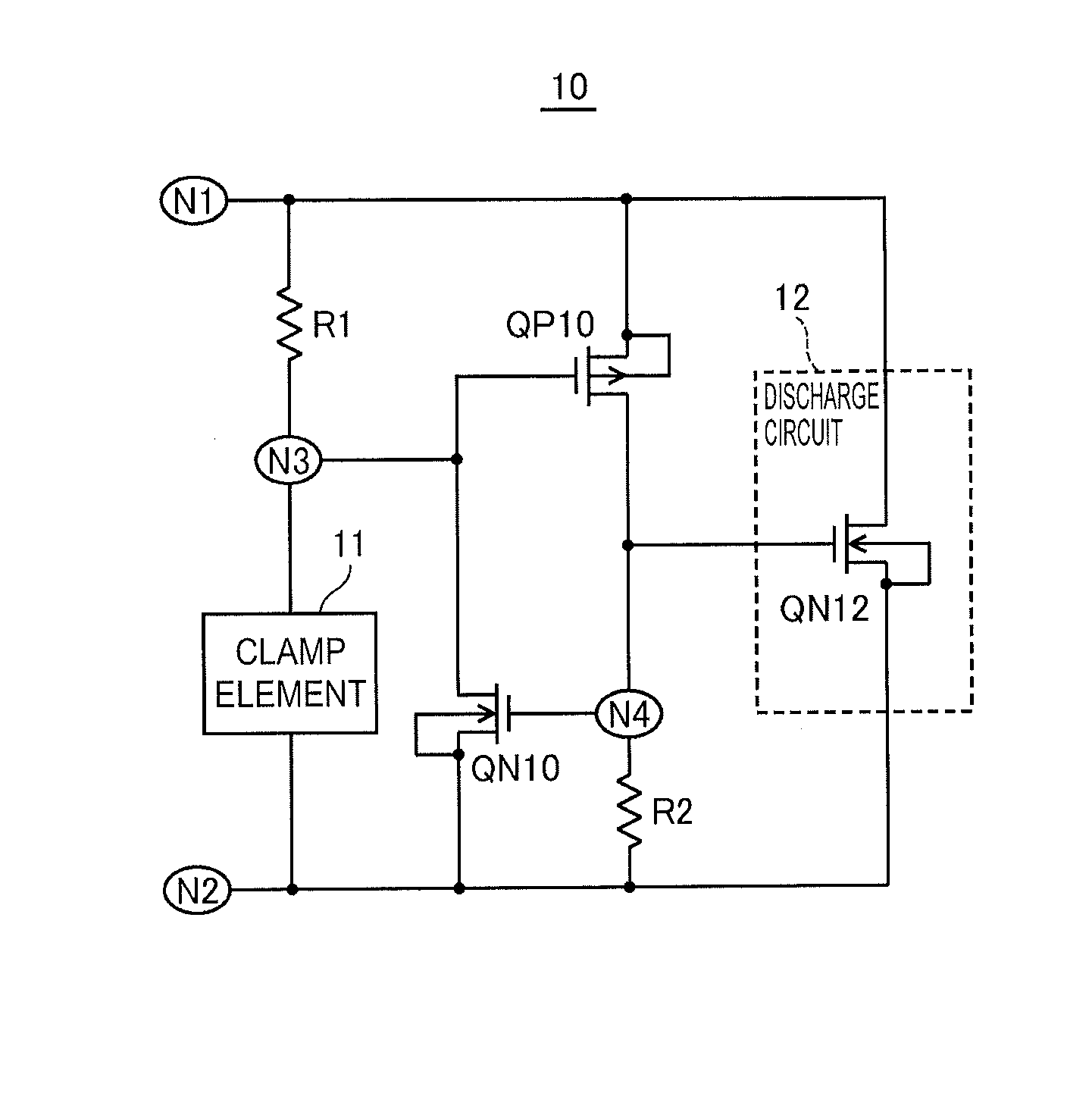
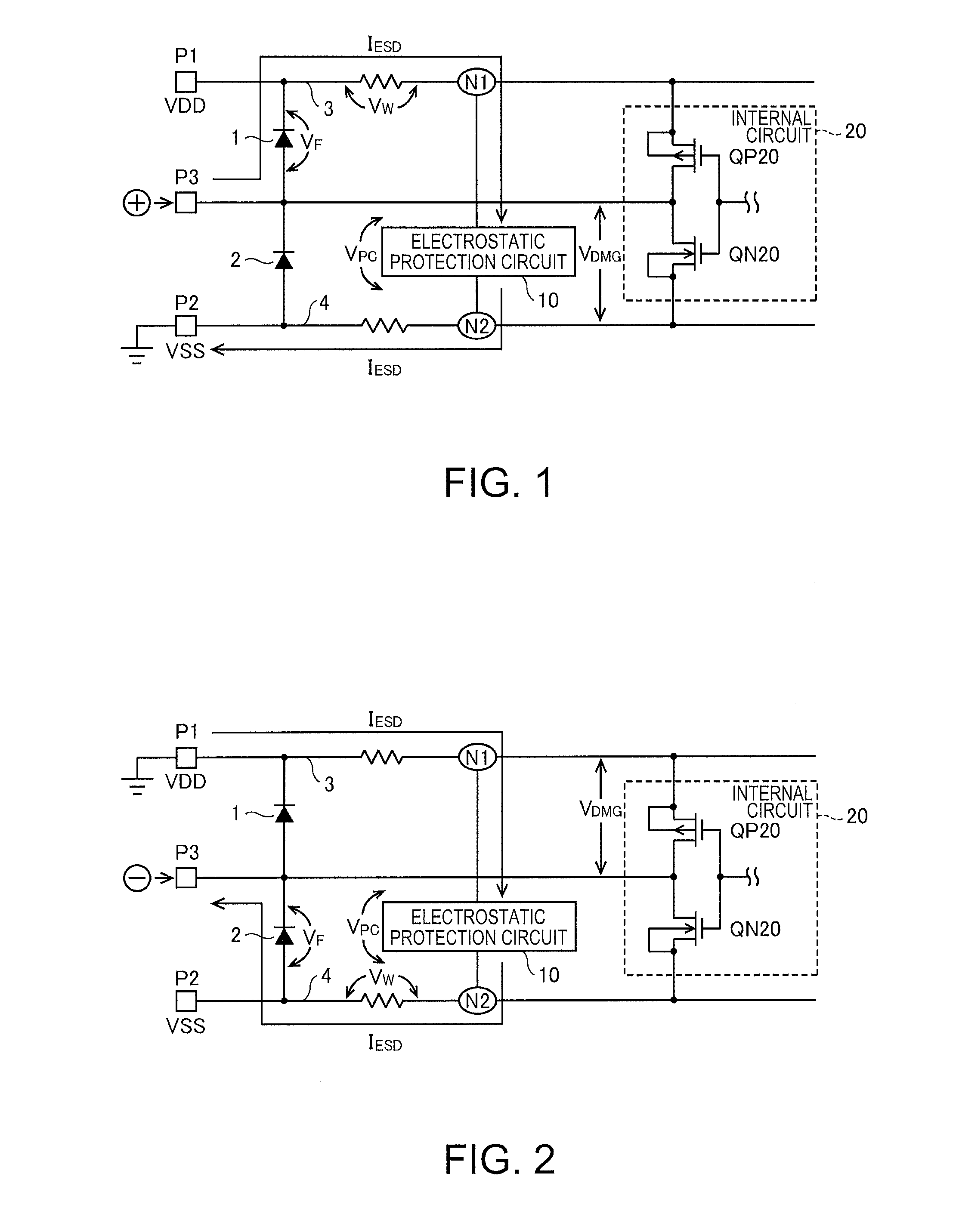
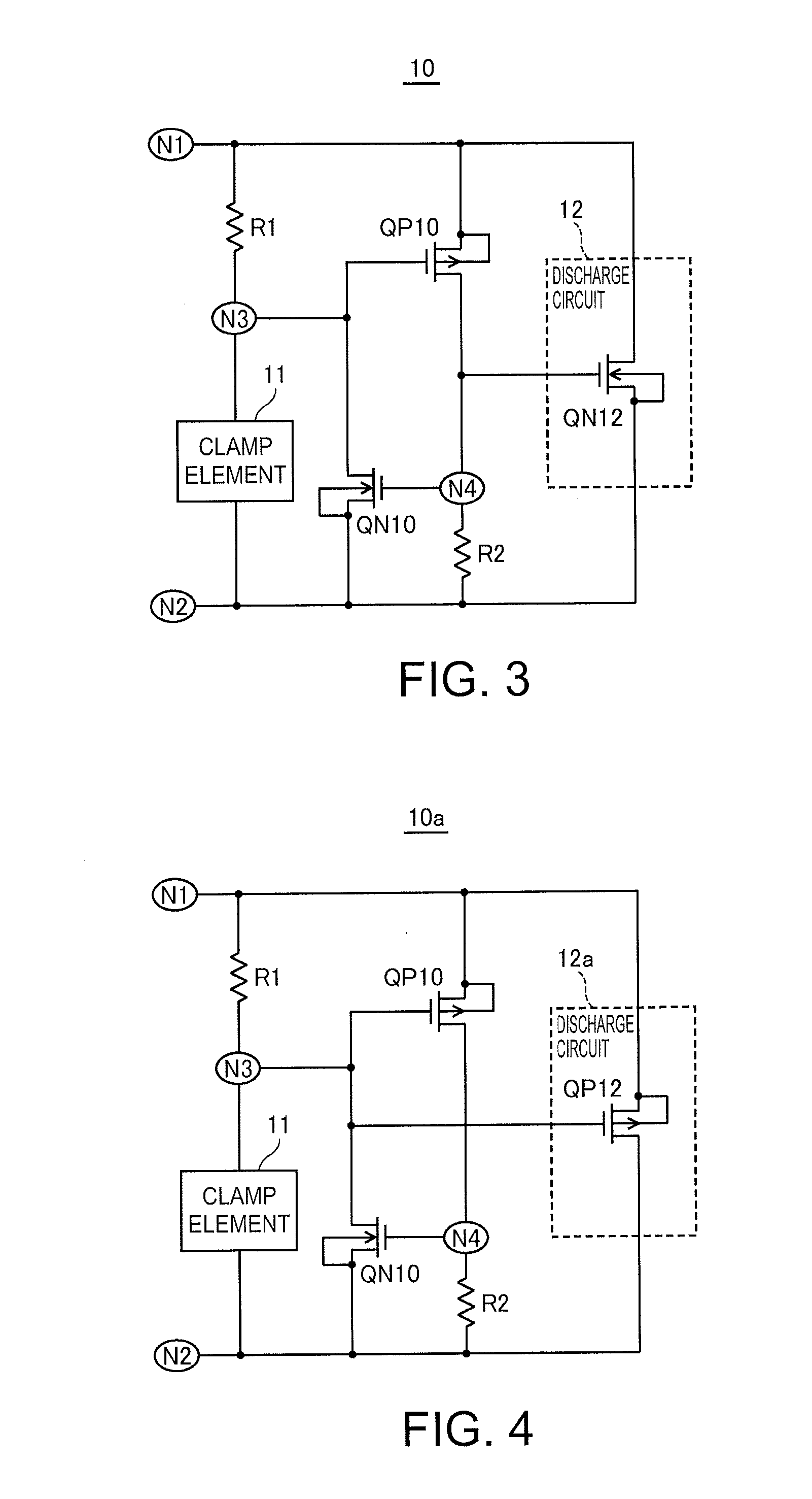
[0065]FIG. 3 is a circuit diagram showing an example of a configuration of an electrostatic protection circuit according to a first embodiment of the invention. As shown in FIG. 3, an electrostatic protection circuit 10 includes resistor elements R1 and R2 as first and second impedance elements, a clamp element 11, a P-channel MOS transistor QP10 as a first transistor, an N-channel MOS transistor QN10 as a second transistor, and a discharge circuit 12.

[0066]The electrostatic protection circuit 10 is connected via a node N1 to a first terminal to which a potential of a high-potential side is supplied, and is connected via a node N2 to a second terminal to which a potential of a low-potential side is supplied. A series circuit including the resistor element R1 and the clamp element 11, which are connected to each other by a node N3, is connected between the node N1 and the node N2. In the present embodiment, the resistor element R1 is connected between the node N1 and the node N3, and...

second embodiment

[0080]FIG. 4 is a circuit diagram showing an example of a configuration of an electrostatic protection circuit according to a second embodiment of the invention. In an electrostatic protection circuit 10a according to the second embodiment, a discharge circuit 12a is used in place of the discharge circuit 12 of the electrostatic protection circuit 10 according to the first embodiment shown in FIG. 3. In other regards, the electrostatic protection circuit 10a shown in FIG. 4 is similar to the electrostatic protection circuit 10 shown in FIG. 3.

[0081]The discharge circuit 12a includes, for example, a P-channel MOS transistor QP12. The transistor QP12 has a source, a drain, and a gate that are connected to a node N1, a node N2, and a node N3, respectively. The discharge circuit 12a allows current to flow from the node N1 to the node N2 in accordance with voltage generated in a resistor element R1 when a transistor QN10 is in an on state.

[0082]A description is now given of an operation ...

third embodiment

[0091]FIG. 5 is a circuit diagram showing an example of a configuration of an electrostatic protection circuit according to a third embodiment of the invention. As compared to the electrostatic protection circuit 10 according to the first embodiment shown in FIG. 3, an electrostatic protection circuit 10b according to the third embodiment additionally includes a detection circuit 13. In other regards, the electrostatic protection circuit 10b shown in FIG. 5 is similar to the electrostatic protection circuit 10 shown in FIG. 3.

[0092]The detection circuit 13 activates an output signal upon detection of an on state of a transistor QN10. For example, the detection circuit 13 includes an inverter composed of a P-channel MOS transistor QP13 and an N-channel MOS transistor QN13. The transistor QP13 has a source, a drain, and a gate that are connected to a node N1, an output terminal OUT, and an input terminal IN, respectively. The transistor QN13 has a drain, a source, and a gate that are ...


PUM


Abstract

The present electrostatic protection circuit includes: a series circuit that is connected between a first node and a second node and includes a first impedance element and a clamp element connected to each other by a third node; a first transistor that is connected between the first node and a fourth node and turns on in accordance with an increase in voltage generated in the first impedance element; a second impedance element connected between the fourth node and the second node; a second transistor that turns on in accordance with an increase in voltage generated in the second impedance element, and increases current flowing in the first impedance element; and a discharge circuit that allows current to flow from the first node to the second node when the second transistor is in an on state.

Description

BACKGROUND[0001]1. Technical Field[0002]The present invention relates to an electrostatic protection circuit for protecting a semiconductor integrated circuit apparatus from electrostatic discharge (ESD). The invention further relates to a semiconductor integrated circuit apparatus embedded with such an electrostatic protection circuit.[0003]2. Related Art[0004]A semiconductor integrated circuit apparatus may be provided with an electrostatic protection circuit to prevent destruction of an internal circuit caused by static electricity. In general, an electrostatic protection circuit is connected between a first terminal to which a potential of a high-potential side is supplied and a second terminal to which a potential of a low-potential side is supplied. For example, when a positive electric charge is applied to the first terminal due to electrostatic discharge, the positive electric charge is discharged to the second terminal via the electrostatic protection circuit. In this case,...

Claims


Application Information

Patent Timeline
IPC IPC(8): H02H9/04
CPCH02H9/04H02H9/046
Inventor IKEDA, MASUHIDE
Owner SEIKO EPSON CORP
Why Eureka
Try Eureka