Semiconductor apparatus and method for producing the same
- Summary
- Abstract
- Description
- Claims
- Application Information
AI Technical Summary
Benefits of technology
Problems solved by technology
Method used
Image

Examples
example
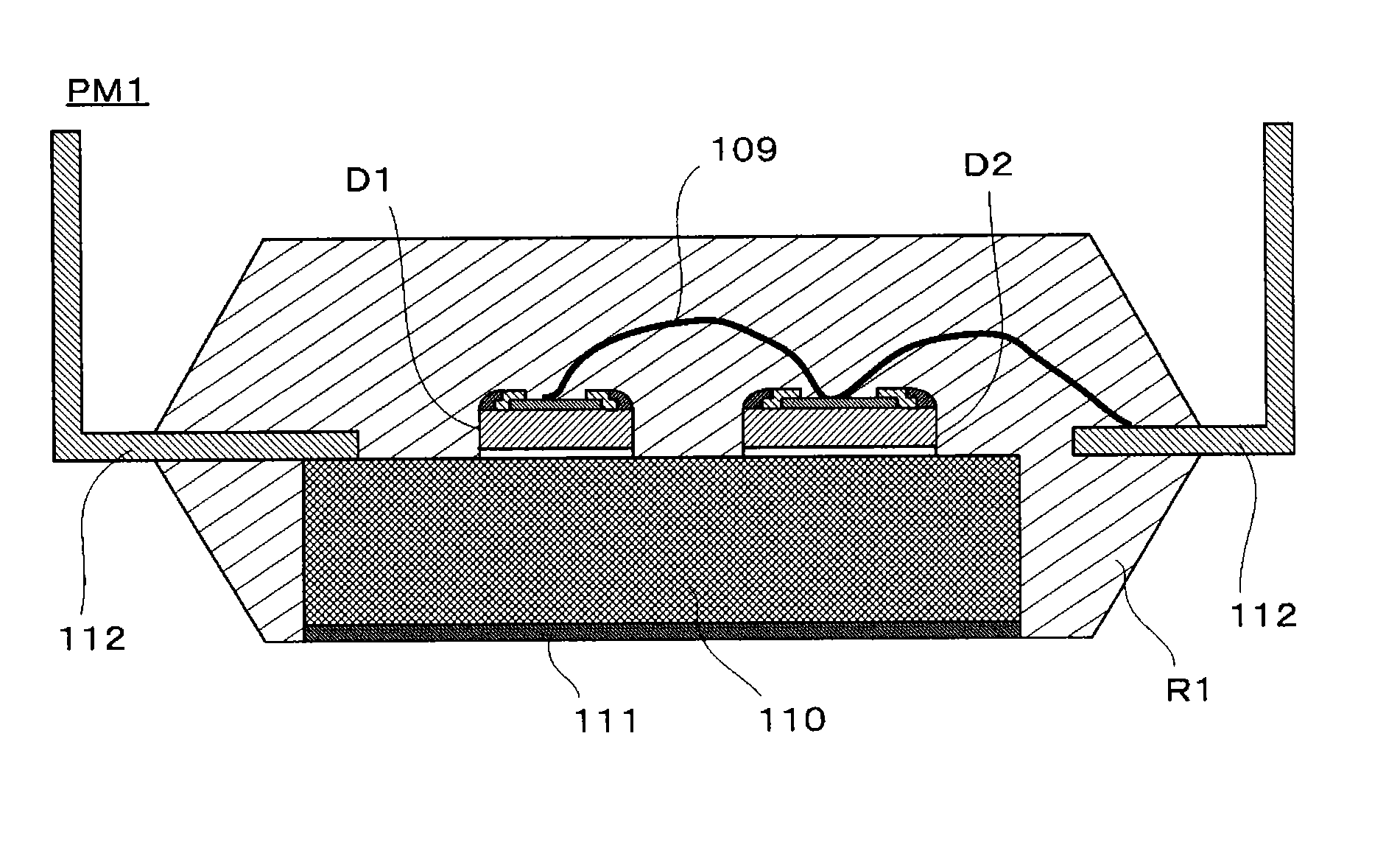
[0052]FIG. 9 is a cross section of a structure of a semiconductor apparatus PM1 of an example of the present invention. Semiconductor apparatus PM1 is a power module with a first semiconductor device 1 and a second semiconductor device D2 connected in parallel, and has a basic configuration similar to that shown in FIG. 1. First semiconductor device 1 and second semiconductor device D2 each include a major electrode, an insulating layer, and a covering layer, and are bonded via solder, sinterable, fine metal particles, or a similar bonding material to a heat spreader 110 that is to serve as the electrically conductive member. Furthermore, semiconductor apparatus PM1 includes a lead frame 112 also serving as a terminal member for an external circuit, with a lead member that is a wire 109 of aluminum ultrasonically bonded and thus connected to semiconductor devices 1 and D2. Wire 109 has one end connected to lead frame 112. Semiconductor apparatus PM1 excluding an external terminal po...
PUM
 Abstract
Description
Claims
Application Information