Nitride semiconductor light emitting element and method for manufacturing same

a technology of light emitting elements and semiconductors, applied in semiconductor/solid-state device manufacturing, semiconductor devices, electrical devices, etc., can solve the problems of disadvantageous lowering of luminous efficiency and lowering of power efficiency per unit power, and achieve the effect of reducing the decrease of luminous efficiency and substantially constant luminous efficiency

Active Publication Date: 2015-06-18
SHARP FUKUYAMA LASER CO LTD
View PDF6 Cites 20 Cited by
  • Summary
  • Abstract
  • Description
  • Claims
  • Application Information

AI Technical Summary

Benefits of technology

[0014]The present invention is made in view of the forgoing problem, and an object of the present invention is to provide a nitride semiconductor light emitting element that can reduce the decrease in luminous efficiency when it is driven at a high temperature or when it is driven with a high current and a method of manufacturing such a nitride semiconductor light emitting element.
[0029]In the configuration of the present invention, especially if the drive temperature is varied, the luminous efficiency remains substantially constant. Thus, it is possible to provide a nitride semiconductor light emitting element that can reduce the decrease in luminous efficiency when it is driven at a high temperature or when it is driven with a high current and a method of manufacturing such a nitride semiconductor light emitting element.

Problems solved by technology

However, when the conventional nitride semiconductor light emitting element is driven with a high current at a high temperature, its luminous efficiency is disadvantageously lowered.
This may cause the power efficiency per unit power to be lowered.

Method used


Image

  • Nitride semiconductor light emitting element and method for manufacturing same
  • Nitride semiconductor light emitting element and method for manufacturing same
  • Nitride semiconductor light emitting element and method for manufacturing same

Examples


example 1

[0152 of the present embodiment will then be described specifically. The present embodiment is not limited to Examples that will be described below.

[0153]A process of manufacturing the nitride semiconductor light emitting element 1 of Example 1 is as described below.

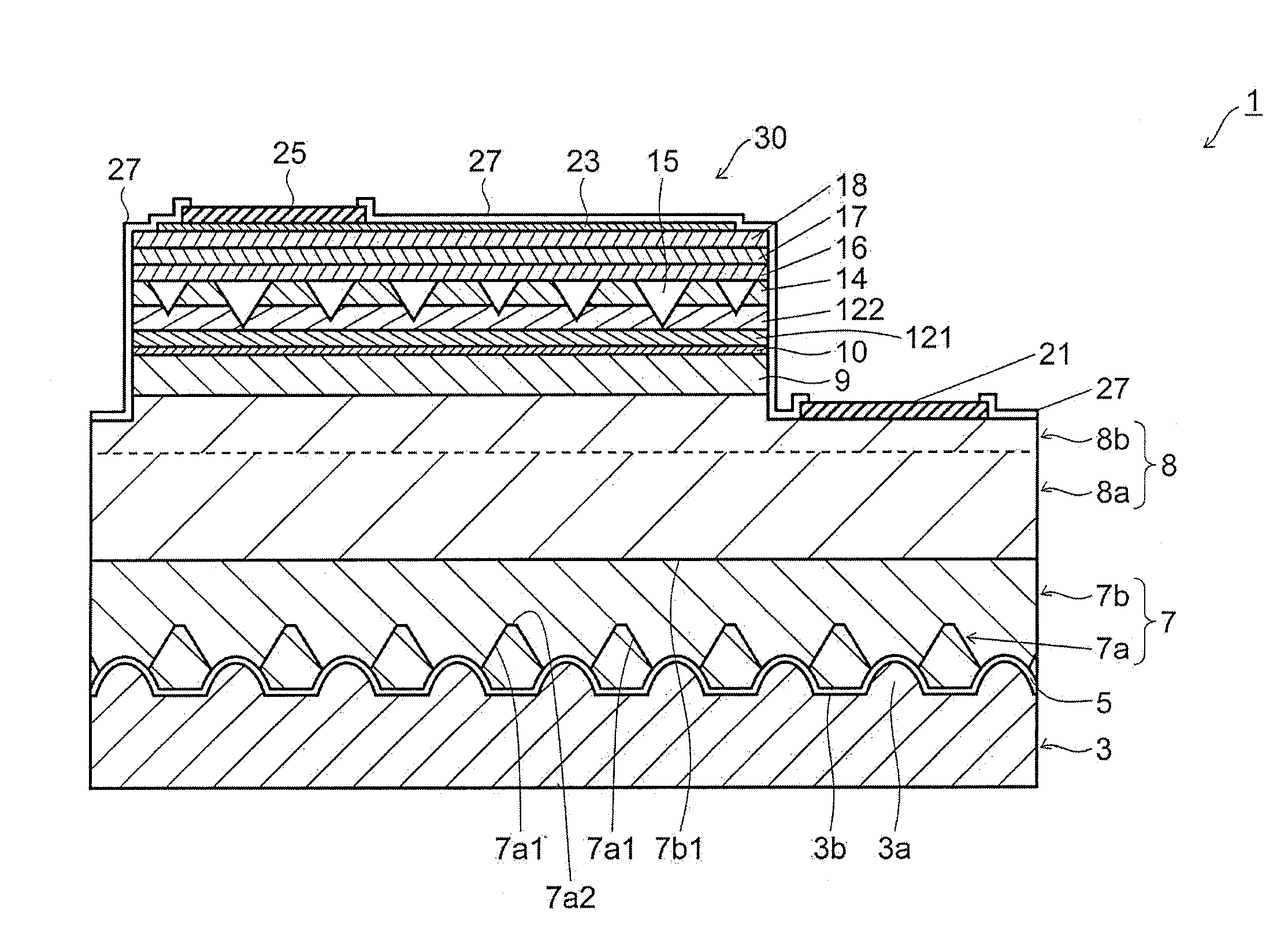
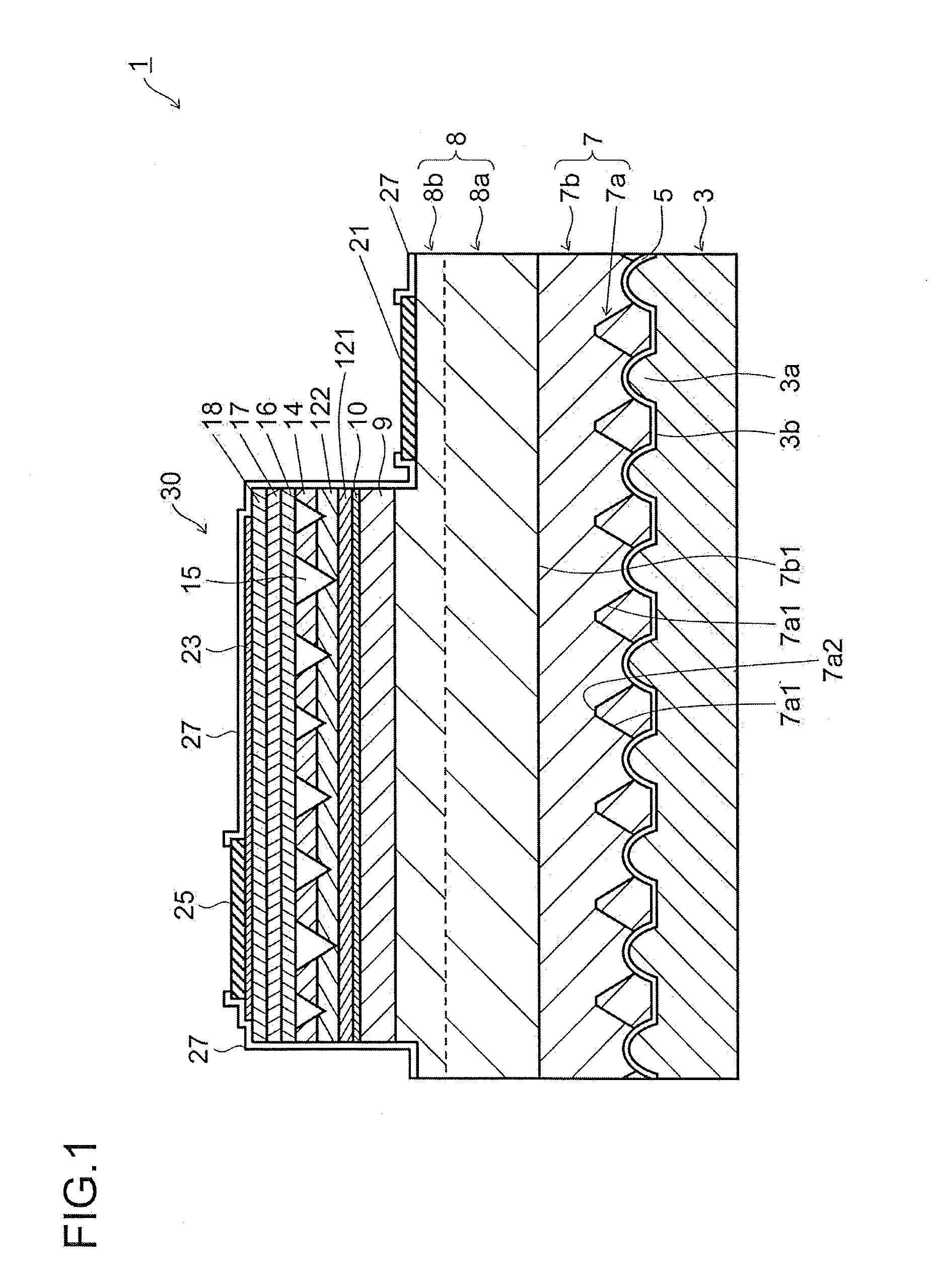
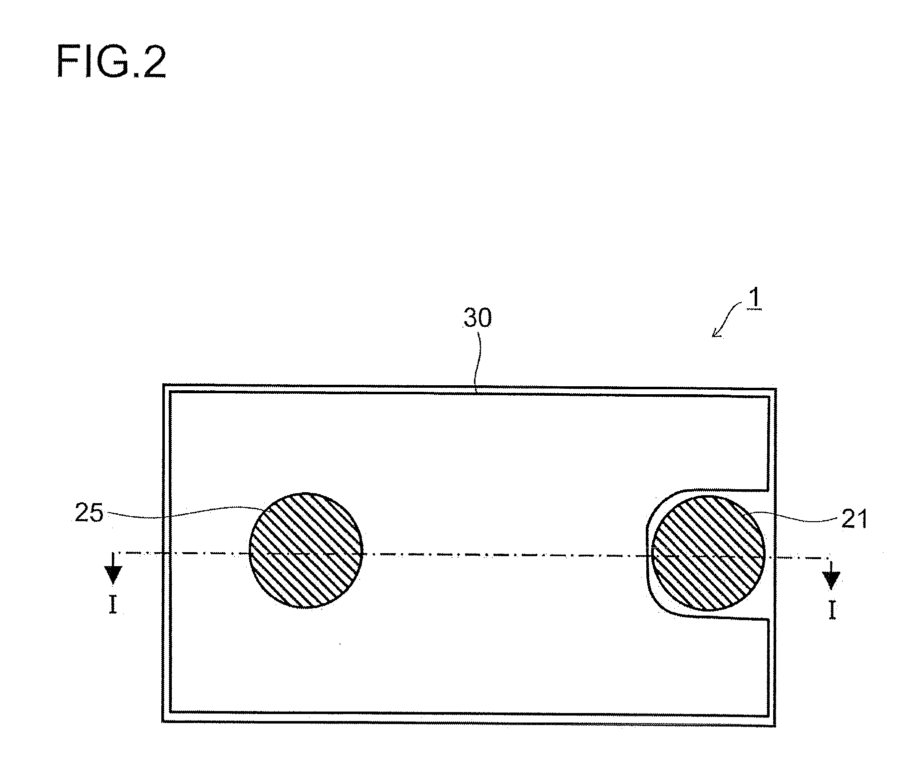
[0154]First, a wafer of a sapphire substrate 3 whose upper surface was subjected to concave and convex processing of convex portions 3A and concave portions 3B and which had a diameter of 100 mm was prepared. The convex portion 3A was substantially circular in plan view, and three adjacent convex portions 3A were arranged so as to be located on the apexes of a substantially regular triangle in plan view. The distance between the adjacent three convex portions 3A was 2 μm.

[0155]The concave and convex processing method of the substrate 3 will be described in detail. On the substrate 3, a mask that defined the planar arrangement of the convex portions 3A shown in FIG. 4 was formed. Then, this mask was used to dry-etch the s...


PUM

PropertyMeasurementUnit
current densityaaaaaaaaaa
thicknessaaaaaaaaaa
thicknessaaaaaaaaaa

Abstract

A nitride semiconductor light emitting element is provided with: a substrate; a buffer layer that is provided on the substrate; a base layer that is provided on the buffer layer; an n-side nitride semiconductor layer that is provided on the base layer; an MQW light emitting layer that is provided on the n-side nitride semiconductor layer; and a p-side nitride semiconductor layer that is provided on the MQW light emitting layer. An x-ray rocking curve half-value width ω (004) with respect to a (004) plane, i.e., the crystal plane of the nitride semiconductor, is 40 arcsec or less, or the x-ray rocking curve half-value width ω (102) with respect to a (102) plane is 130 arcsec or less, and the rate P (80) / P (25) between light output P (25) at 25° C. and light output P (80) at 80° C. with a same operating current is 95% or more.

Description

CROSS-REFERENCE TO RELATED APPLICATIONS[0001]This application is a national phase filing under 35 U.S.C. §371 of International Application No. PCT / JP2013 / 063482, filed on May 15, 2013, and which claims priority to Japanese Patent Application No. 2012-133489, filed on Jun. 13, 2012, the contents of which prior applications are incorporated herein by reference.FIELD OF THE INVENTION[0002]The present invention relates to a nitride semiconductor light emitting element and a method of manufacturing such a nitride semiconductor light emitting element.BACKGROUND OF THE INVENTION[0003]A III-V compound semiconductor material containing nitrogen (hereinafter referred to as a “nitride semiconductor material”) has a band gap corresponding to the energy of light having wavelengths from the infrared region to the ultraviolet region. Hence, the nitride semiconductor material is useful for the material of a light emitting element that emits light having wavelengths from the infrared region to the u...

Claims


Application Information

Patent Timeline
Patent Type & Authority Applications(United States)
IPC IPC(8): H01L33/00H01L33/24H01L33/32H01L33/12H01L33/06
CPCH01L33/0075H01L33/0025H01L33/12H01L2933/0033H01L33/32H01L33/24H01L33/06H01L33/007H01L33/20H01L33/22H01L33/025
Inventor NAKATSU, HIROSHIINOUE, TOMOYANONAKA, KENTAROASAI, TOSHIAKITAKEOKA, TADASHITANI, YOSHIHIKO
Owner SHARP FUKUYAMA LASER CO LTD
Why Eureka
Try Eureka