Fluorine Passivation of Dielectric for Superconducting Electronics

a superconducting electronics and fluorine technology, applied in the direction of superconducting magnets/coils, magnetic bodies, and semiconductor/solid-state device details, can solve the problems of many surface treatments ineffective to remove defects from the bulk of the film, loss tangent, and unwanted reactions between the dielectric and the wiring materials

Inactive Publication Date: 2015-06-25
INTERMOLECULAR
View PDF0 Cites 18 Cited by
  • Summary
  • Abstract
  • Description
  • Claims
  • Application Information

AI Technical Summary

Benefits of technology

[0006]Embodiments of superconducting circuits include an a-Si ILD passivated with fluorine (F) throughout its bulk as well as at its interfaces. The ILD is deposited and flu...

Problems solved by technology

The loss tangent is believed to be caused by defects occurring during deposition.
However, crystallization of interlayer dielectrics for superconducting circuits typically requires temperatures high enough to cause unwanted reactions between the dielectric and the wiring materials (e.g., Al or Nb).
At this thickness, many surfac...

Method used


Image

  • Fluorine Passivation of Dielectric for Superconducting Electronics
  • Fluorine Passivation of Dielectric for Superconducting Electronics
  • Fluorine Passivation of Dielectric for Superconducting Electronics

Examples


Embodiment Construction

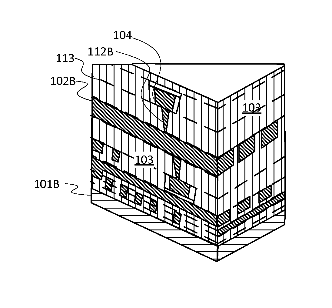
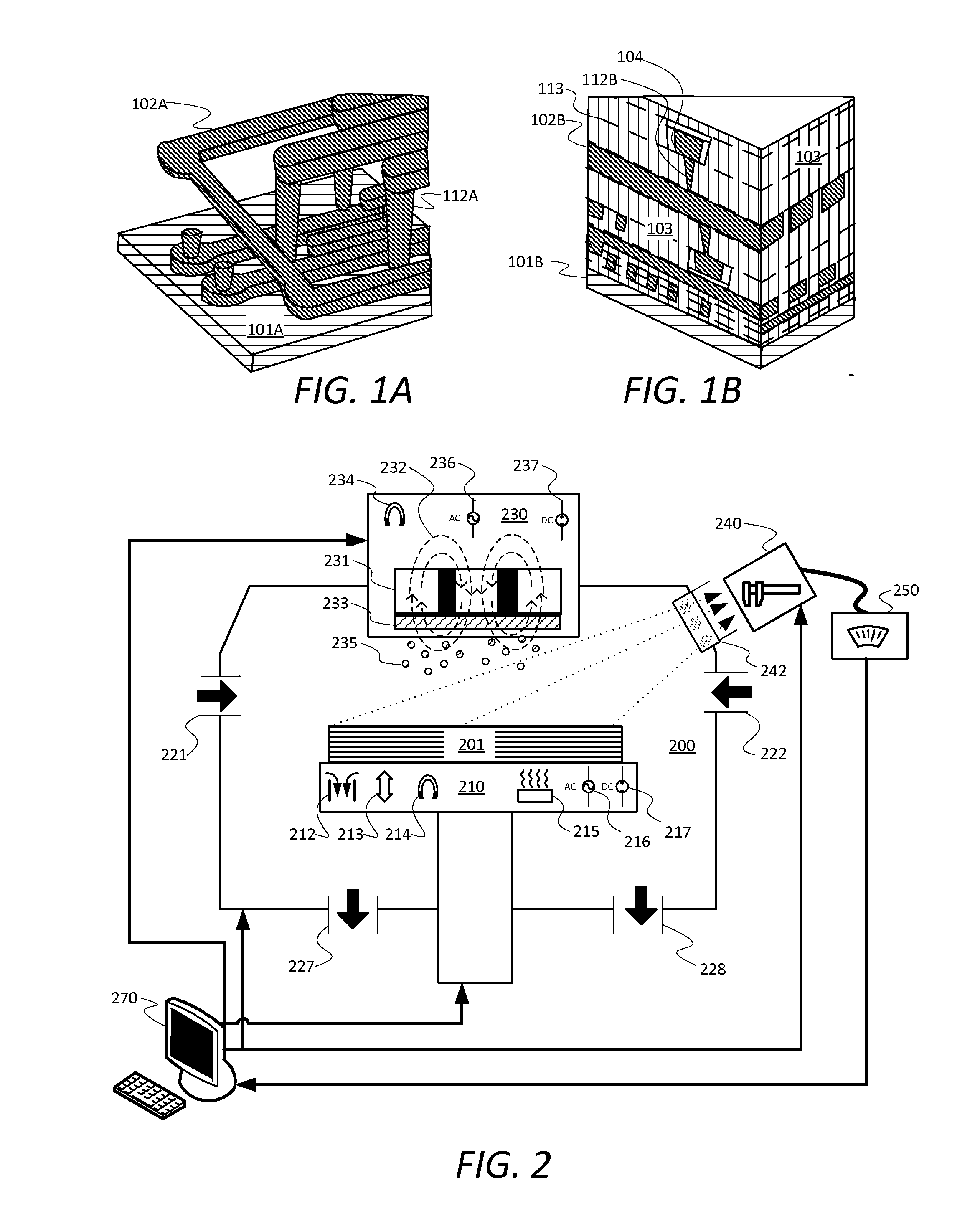
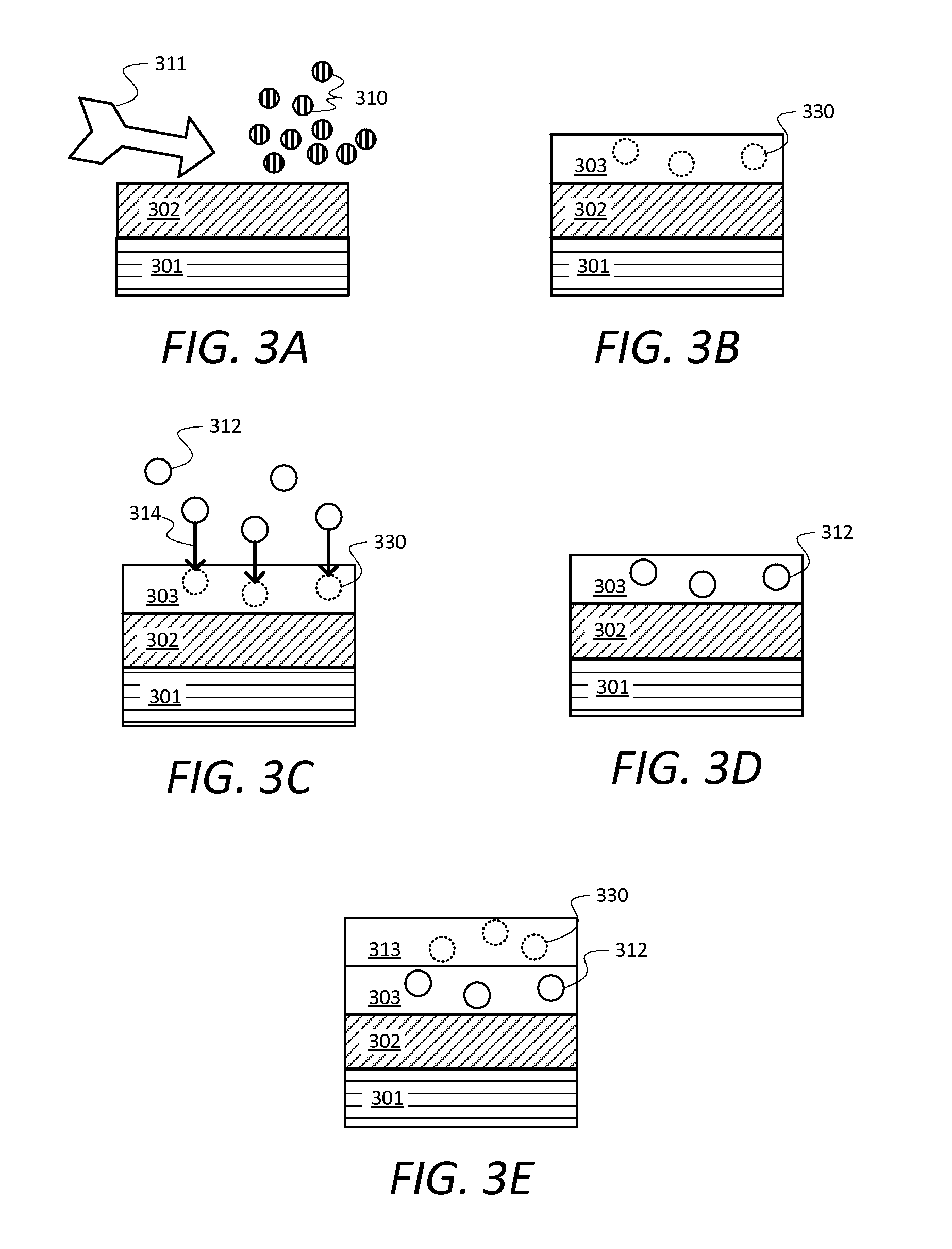
[0016]A detailed description of one or more example embodiments is provided below. To avoid unnecessarily obscuring the description, some technical material known in the related fields is not described in detail. Semiconductor fabrication generally requires many other processes before and after those described; this description omits steps that are irrelevant to, or that may be performed independently of, the described processes.

[0017]Unless the text or context clearly dictates otherwise: (1) by default, singular articles “a,”“an,” and “the” (or the absence of an article) may encompass plural variations; for example, “a layer” may mean “one or more layers.” (2) “Or” in a list of multiple items means that any, all, or any combination of less than all the items in the list may be used in the invention. (3) Where a range of values is provided, each intervening value is encompassed within the invention. (4) “About” or “approximately” contemplates up to 10% variation. “Substantially” con...


PUM

PropertyMeasurementUnit
Temperatureaaaaaaaaaa
Thicknessaaaaaaaaaa
Thicknessaaaaaaaaaa

Abstract

An amorphous silicon (a-Si) dielectric for superconducting electronics is fabricated with reduced loss tangent by fluorine passivation throughout the bulk of the layer. Complete layers or thinner sub-layers of a-Si are formed by physical vapor deposition at low temperatures (<350 C, e.g. ˜200 C) to prevent reaction with superconducting materials, then exposed to fluorine. The fluorine may be a component of a gas or plasma, or it may be a component of an interface layer. The fluorine is driven into the a-Si by heat (e.g., <350 C) or impact to passivate defects such as dangling bonds.

Description

BACKGROUND[0001]Related fields include thin-film microwave devices with superconducting components and passivation processes for dielectrics.[0002]At temperatures <100 mK, amorphous silicon (a-Si) is a dielectric. Its low cost and ease of fabrication make it attractive as an interlayer dielectric (ILD) for superconducting interconnects and components for planar microwave devices, but its loss tangent (˜108) is much larger than that of single-crystal Si (˜107) at microwave frequencies (e.g., 3-300 GHz) and longer infrared frequencies (300-1000 GHz). The loss tangent is believed to be caused by defects occurring during deposition. A lower loss tangent would benefit high-frequency classical devices by reducing signal attenuation, dispersion and jitter. A lower loss tangent would benefit quantum devices, such as rapid single flux quantum (RFSQ) circuits and reciprocal quantum logic (RQL) by increasing coherence times for quantum state signals.[0003]Crystalline dielectrics are observe...

Claims


Application Information

Patent Timeline
IPC IPC(8): H01L39/24C23C14/14C23C14/58H01L39/12
CPCH01L39/24H01L39/249C23C14/5806C23C14/14H01L39/12H01L23/5329H01L21/76826H01L23/53285H01L2924/0002H01L21/76891H01L21/02123H01L21/02266H01L21/02321H01L21/02337H01L21/0234H01L21/3115C23C14/16C23C14/5846Y10T428/265H10N69/00H01L2924/00
Inventor PRAMANIK, DIPANKARSTEINBACH, ANDREW
Owner INTERMOLECULAR
Why Eureka
Try Eureka