Analog-digital converter

a digital converter and analog technology, applied in the field of analog digital converters, can solve the problems of large percentage of power consumption of parallel-type ad converters, power consumption increase, and accuracy deterioration of resistor ladder circuits, so as to suppress the effect of noise current, suppress the effect of bias current, and reduce the bias current

Inactive Publication Date: 2015-06-25
KAGOSHIMA UNIV
View PDF1 Cites 1 Cited by
  • Summary
  • Abstract
  • Description
  • Claims
  • Application Information

AI Technical Summary

Benefits of technology

[0011]According to the present invention, by a correction circuit in a resistor ladder circuit, a variation in comparison reference potential caused by noise currents that comparators generate is corrected, thus making it possible to decrease a bias current in the resistor ladder circuit and to suppress accuracy deterioration in analog-digital conversion. Consequently, it is possible to suppress an effect caused by the noise currents that the comparators generate while suppressing an increase in power consumption, and it becomes possible to provide a low power consumption and high precision analog-digital converter.

Problems solved by technology

On the other hand, in the case of an n-bit parallel-type AD converter (total-bit flash AD converter), for example, (2n−1) pieces of comparators are required and power consumption increases.
However, in recent years, achievement of low power of the comparators advances, and power consumption in the resistor ladder circuit accounts for a large percentage of power consumption of the parallel-type AD converter.
Noises from the comparators CMP1 to CMPm are one of the causes of accuracy deterioration of the resistor ladder circuit.
The variation in the comparison reference potential VREF caused by the noise currents In increases a conversion error in the AD conversion and thereby the accuracy of the parallel-type AD converter deteriorates.
However, when the bias current Ibias in the resistor ladder circuit is set to be sufficiently larger than the noise current In in order to suppress the accuracy deterioration of the parallel-type AD converter as described previously, there is caused a problem that the power consumption in the resistor ladder circuit increases.

Method used


Image

  • Analog-digital converter
  • Analog-digital converter
  • Analog-digital converter

Examples


first embodiment

[0038]There will be explained a first embodiment of the present invention.

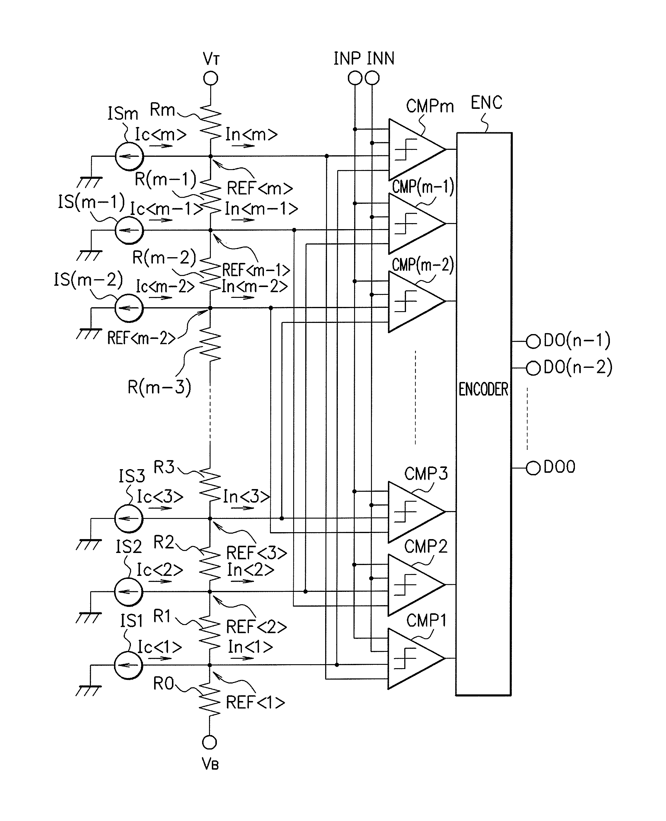
[0039]An AD converter in the first embodiment supplies a current that is the same in magnitude as the noise current In generated by the comparator and flows in a reverse direction to the connection point REF in the resistor ladder circuit corresponding to the output node of the comparison reference potential VREF, to thereby offset the noise current In and suppress the potential variation in the resistor ladder circuit. FIG. 1 is a diagram illustrating a configuration example of an AD converter in the first embodiment. FIG. 1 illustrates a parallel-type AD converter that converts input analog input signals to n-bit (n being a natural number) digital signals DO[n−1:0] (a flash AD converter) as one example. In FIG. 1, R0 to Rm (m=2n−1) represent resistors, and IS1 to ISm represent current sources. Further, CMP1 to CMPm represent comparators (comparators), and ENC represents an encoder.

[0040]The resistors R0 to R...

second embodiment

[0045]Next, there will be explained a second embodiment of the present invention.

[0046]A potential variation ΔV at the connection point REF in the resistor ladder circuit caused by the noise current In that the comparator generates is expressed by (Expression 3).

[0047][Mathematical expression 3]

ΔV<i>=R·Ceff·i(N-i){ΔVq(N+i)-3(Vcom-VB)}3tcCeff=Cp·CsCp+CsΔVq=VT-VBNVcom=VINP+VINN2(Expression3)

[0048]In aforementioned (Expression 3), R represents a resistance value of the resistor configuring the resistor ladder circuit, Cs represents a capacitance value of the sampling capacitor provided in the comparator, and Cp represents a capacitance value of the parasitic capacitor in the comparator. Further, N represents the number of resistors configuring the resistor ladder circuit (the number of potential ranges divided by the comparison reference potentials that the resistor ladder circuit generates), VT represents a reference voltage on the high potential side, VB represents a reference ...

third embodiment

[0057]Next, there will be explained a third embodiment of the present invention.

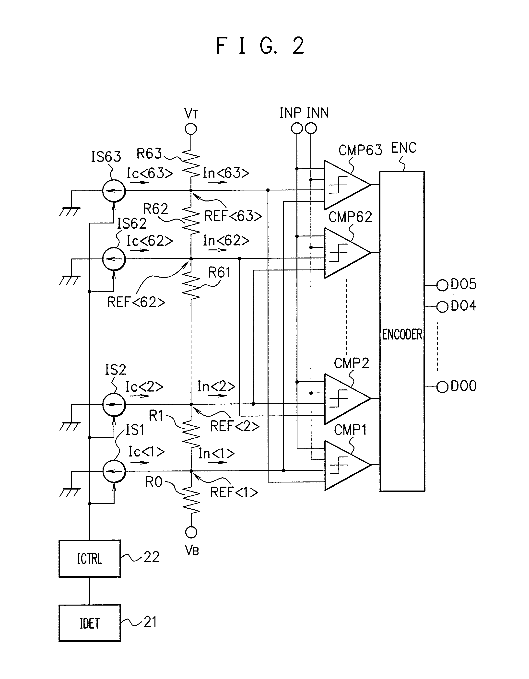
[0058]In the first and second embodiments, for each of the connection points REF1> to REF in the resistor ladder circuit, the current source ISi provided for supplying the correction current Ic is provided, but as described previously, the current source ISi is provided only for the connection point REF where the variation in the potential VREF caused by the noise current In is expected to be large, and thereby it is possible to improve the potential variation in the resistor ladder circuit caused by the noise currents In.

[0059]In the third embodiment to be explained below, the current source ISi is provided for the connection point REF where the variation in the potential VREF in the resistor ladder circuit caused by the noise current In is expected to be large. FIG. 9 is a diagram illustrating a configuration example of an AD converter in the third embodiment. In FIG. 9, for connection points REF posit...


PUM


Abstract

A parallel-type AD converter includes: a plurality of comparators that receive comparison reference potentials different from one another and compare the comparison reference potentials and received analog input signals; an encoder that encodes outputs of the plurality of comparators to output digital signals; and a resistor ladder circuit that resistance-divides a reference voltage to generate the comparison reference potentials and supplies the comparison reference potentials to the comparators through output nodes each positioned between resistors, and is designed to supply a correction current corresponding to noise currents that the comparators generate to the output nodes of the comparison reference potentials in the resistor ladder circuit, and thereby the noise currents that the comparators generate are offset by the correction current, a bias current in the resistor ladder circuit can be decreased, and accuracy deterioration in AD conversion can be suppressed.

Description

TECHNICAL FIELD[0001]The present invention relates to an analog-digital converter (AD converter).BACKGROUND ART[0002]FIG. 6A is a diagram illustrating a configuration example of a parallel-type analog-digital converter (AD converter). FIG. 6A illustrates a parallel-type AD converter (flash AD converter) that converts input analog input signals to n-bit (n being a natural number) digital signals DO[n−1:0]. In FIG. 6A, R0 to Rm (m=2n−1) represent resistors, CMP1 to CMPm represent comparators (comparators), and ENC represents an encoder.[0003]The resistors R0 to Rm are connected in series between a power supply terminal to which a reference voltage VB on the low potential side is supplied and a power supply terminal to which a reference voltage VT on the high potential side is supplied in the order of the resistors R0, R1, R2, . . . , R(m−3), R(m−2), R(m−1), and Rm. With i being an integer of 1 to m, a potential at a connection point REF between the resistor R(i−1) and the resistor Ri ...

Claims


Application Information

Patent Timeline
Patent Type & Authority Applications(United States)
IPC IPC(8): H03M1/00H03M1/08H03M1/36
CPCH03M1/002H03M1/361H03M1/0845H03M1/1225H03M7/165H03M1/00H03M1/12G02F7/00H03M1/0612H03M1/145H03M1/365H03M1/0607
Inventor OHHATA, KENICHI
Owner KAGOSHIMA UNIV
Why Eureka
Try Eureka