Common mode filter

a filter and common mode technology, applied in the field of common mode filters, can solve the problems of increasing the transmission loss of a signal, reducing the self-resonant frequency, and requiring a small transmission loss, so as to reduce the unnecessary capacitance, reduce the effect of variation and space saving

Active Publication Date: 2015-07-30
MURATA MFG CO LTD
View PDF9 Cites 19 Cited by
  • Summary
  • Abstract
  • Description
  • Claims
  • Application Information

AI Technical Summary

Benefits of technology

[0015]The first inductance element, the second inductance element, the first resonant circuit, and the second resonant circuit preferably are integrated in a laminate including a plurality of base material layers laminated on each other. This provides a common mode filter in a limited space and achieves space saving.
[0016]The first inductance element and the second inductance element each preferably include an inductor electrode, the first capacitance element and the second capacitance element each preferably include a capacitor electrode, and the inductor electrode preferably is surrounded by the capacitor electrode. With such a configuration, even if another external electronic co

Problems solved by technology

However, as the inductance value of a coil is increased and a coupling coefficient between coils is increased, a self-resonant frequency is decreased and the transmission loss of a signal is also increased.
Therefore, it is difficult to use such a com

Method used


Image

  • Common mode filter
  • Common mode filter
  • Common mode filter

Examples


first preferred embodiment

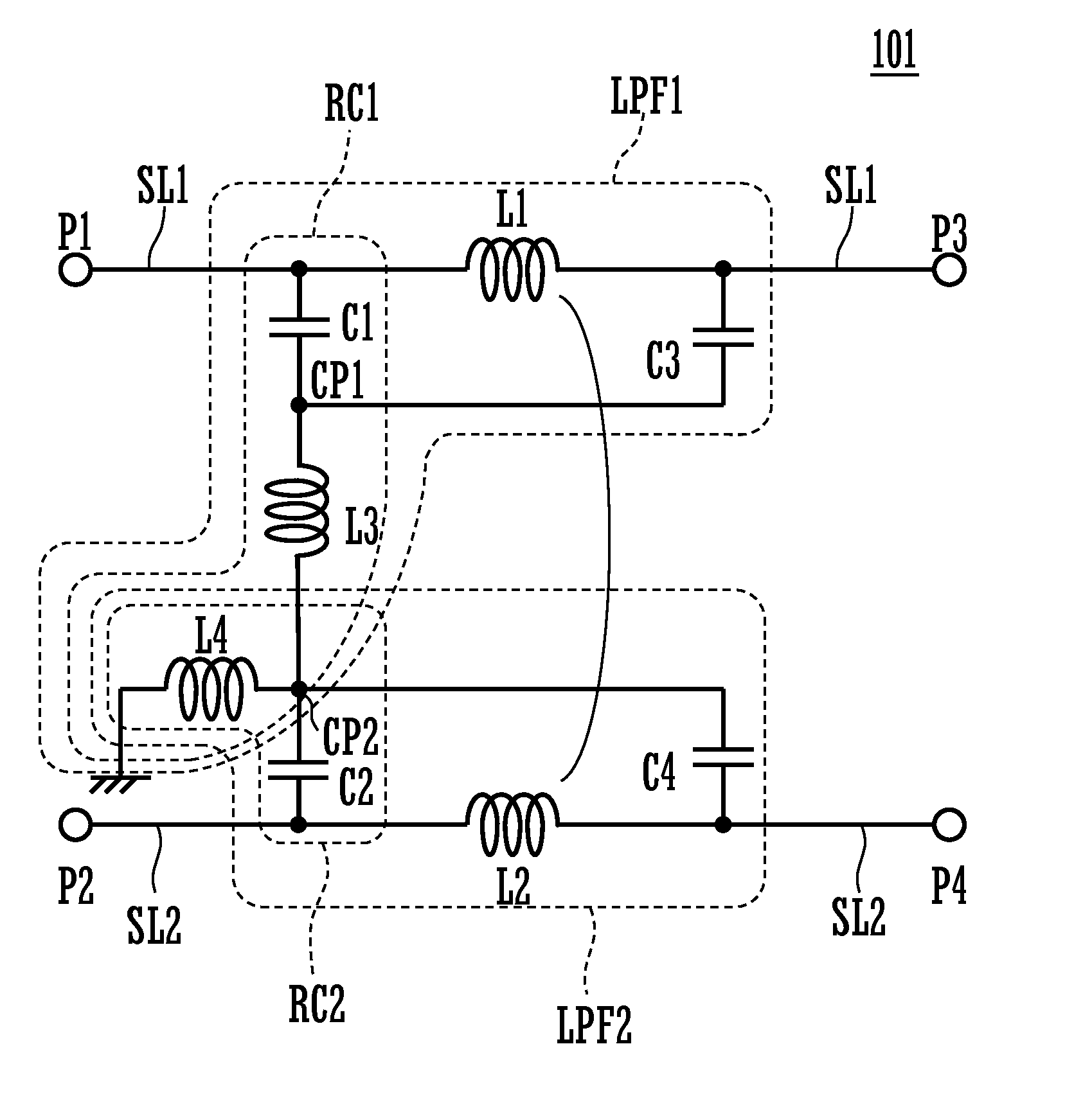
[0037]A common mode filter according to a first preferred embodiment of the present invention will be described with reference to the drawings. FIG. 1 is a circuit diagram of a common mode filter 101 according to the first preferred embodiment of the present invention.

[0038]The common mode filter 101 preferably includes a differential transmission line including a first signal line SL1 and a second signal line SL2 between a port (P1, P2) and a port (P3, P4). The first signal line SL1 includes a first inductance element (hereinafter referred to as a “first inductor”) L1 arranged in series, and the second signal line SL2 includes a second inductance element (hereinafter referred to as a “second inductor”) L2 arranged in series. In addition, the common mode filter 101 preferably includes a ground as a reference with respect to the first signal line SL1 and the second signal line SL2. Moreover, the common mode filter 101 also preferably includes a first resonant circuit RC1 arranged bet...

second preferred embodiment

[0069]A common mode filter according to a second preferred embodiment of the present invention will be described with reference to the drawings. The circuit diagram of the common mode filter 102 according to the second preferred embodiment is the same as the circuit diagram shown in FIG. 1 in the first preferred embodiment.

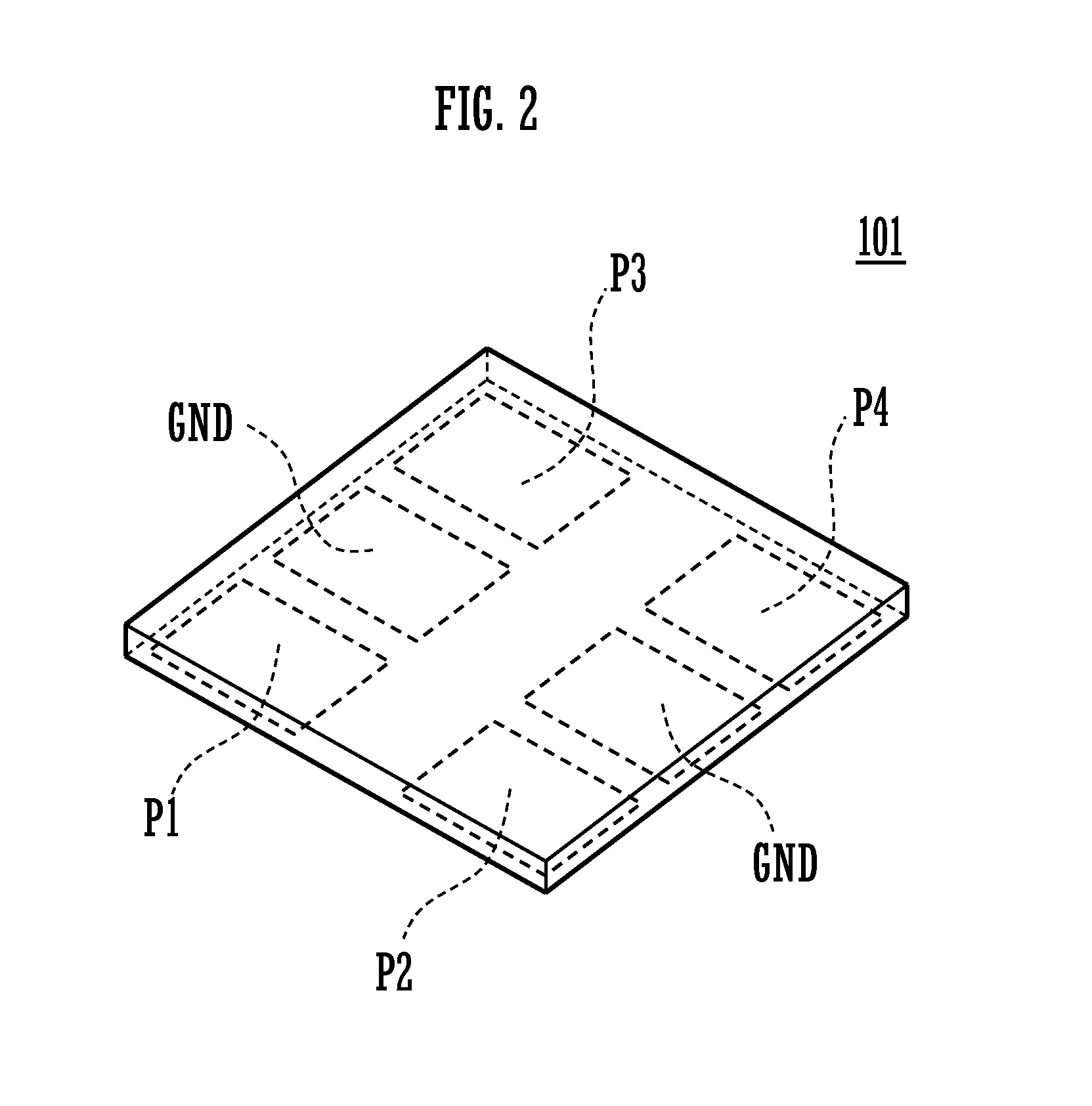
[0070]FIG. 6 is an appearance perspective view of the common mode filter 102. The common mode filter 102 is a laminate of the base material layers including various conductor patterns to be described below. The common mode filter 102 includes ports P1 to P4 and a ground terminal GND on the bottom surface of the common mode filter 102.

[0071]FIG. 7 is a plan view of pre-laminated base material layers of a laminate that defines the common mode filter 102. The common mode filter 102 is a laminate of four base material layers BML1 to BML4 including various conductor patterns. The base material layers BML1 to BML4 are resin sheets, and the base material layer BML1 is th...

third preferred embodiment

[0090]FIG. 9 is a circuit diagram of a common mode filter 103 according to a third preferred embodiment of the present invention. While the common mode filter 103 has a basic circuit configuration similar to the circuit configuration of the common mode filter 101 shown in FIG. 1 in the first preferred embodiment, the first inductor L1 and the second inductor L2 are not positively coupled to each other in a magnetic field. In other words, the first inductor L1 and the second inductor L2 do not act as a common mode choke coil.

[0091]Even in such a common mode filter 103, the first capacitor C1, the third inductor L3, and the fourth inductor L4 define a first resonant circuit RC1, and the second capacitor C2 and the fourth inductor L4 define a second resonant circuit RC2. In addition, the inductors L1 and L2 and the capacitors C1, C3, C2, and C4 mainly define a low pass filter. Therefore, the first resonant circuit RC1 and the second resonant circuit RC2 prevent the common mode noise fr...


PUM


Abstract

A common mode filter includes, between ports, a differential transmission line including a first signal line and a second signal line. The first signal line includes a first inductor arranged in series, and the second signal line includes a second inductor arranged in series. In addition, a first resonant circuit is provided between the first end of the first inductor and the ground, and a second resonant circuit is provided between the first end of the second inductor and the ground.

Description

BACKGROUND OF THE INVENTION[0001]1. Field of the Invention[0002]The present invention relates to a common mode filter that significantly reduces common mode noise that propagates through a transmission line.[0003]2. Description of the Related Art[0004]In order to significantly reduce common mode noise that is to propagate through a differential transmission line, a common mode choke coil has been conventionally used. The common mode choke coil, as described in Japanese Unexamined Patent Application Publication No. 2003-133135, for example, includes two coils that are configured so that a magnetic field generated in each of the coils is canceled out by a differential mode signal (normal mode signal) and the magnetic field is increased with respect to a common mode signal (common mode noise).[0005]In general, such a common mode choke coil is required that each coil has a large inductance value and that a coupling coefficient between the coils is large.[0006]However, as the inductance ...

Claims


Application Information

Patent Timeline
IPC IPC(8): H03H7/01
CPCH03H7/0115H03H7/09H03H2001/0085H03H7/427H03H7/1725H03H7/1783H03H7/1733H03H7/1775H03H7/1758H01P1/20
Inventor YOSUI, KUNIAKIKATO, NOBORUAKIYAMA, HISASHI
Owner MURATA MFG CO LTD
Why Eureka
Try Eureka