Method and apparatus for forming fine scale structures in dielectric substrate

a dielectric substrate and fine scale technology, applied in the direction of laser beam welding apparatus, lithographic mask, laser beam welding process, etc., can solve the problems of slow direct write process, difficult control of depth to high precision over all features, and difficulty in maintaining constant depth at the intersection of grooves and pads

Active Publication Date: 2015-08-13
M SOLV LTD
View PDF1 Cites 6 Cited by
  • Summary
  • Abstract
  • Description
  • Claims
  • Application Information

AI Technical Summary

Benefits of technology

[0014]The choice of laser enables the scanning to be carried out at high speed so the structures can be formed in a short time period whilst avoiding the need for high capital cost and / or high operating costs. The process also allows each of the process steps for forming the different types of structures to be separately optimised.

Problems solved by technology

However, because of the limited laser power available from highly focusable UV DPSS lasers, this direct write process is slow when it comes to removing the more substantial volume of material associated with the larger area pads and ground planes.
This direct write method also has difficulty maintaining constant depth at the intersections between grooves and pads.
However, due to ablation rate dependence on structure size, control of depth to high precision over all features is often difficult.
Except in the case where the circuitry is extremely dense, this mask imaging approach is also significantly more costly than the direct write approach since the purchase and operating costs of excimer lasers are both very high.
Mask imaging is also very inflexible in that a new mask needs to be used for each layer of the circuit.
However, it still suffers from the high cost associated with the use of excimer lasers.
Hence, it can be seen that the existing process methods for making advanced circuits based on this “laser-embedded circuit technology” have serious disadvantages.

Method used


Image

  • Method and apparatus for forming fine scale structures in dielectric substrate
  • Method and apparatus for forming fine scale structures in dielectric substrate
  • Method and apparatus for forming fine scale structures in dielectric substrate

Examples


Embodiment Construction

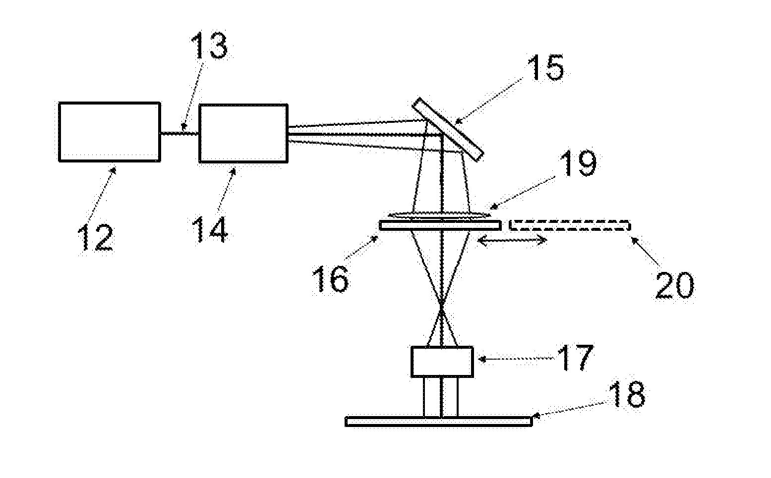
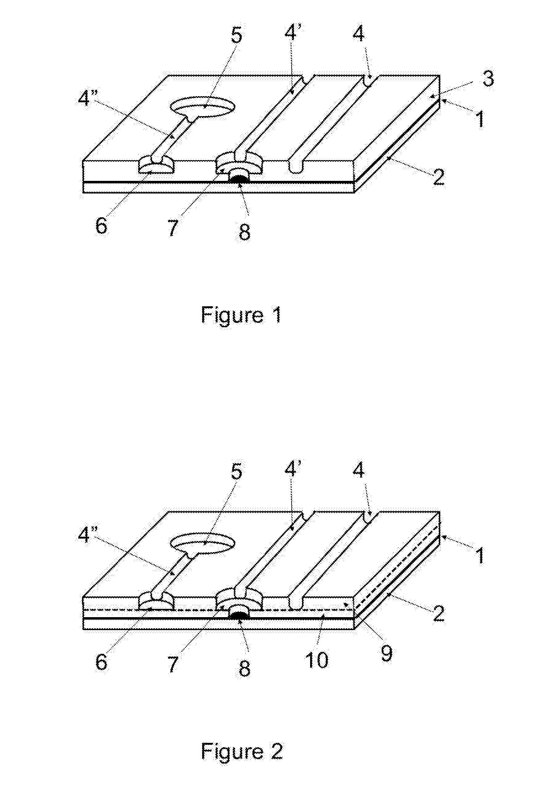
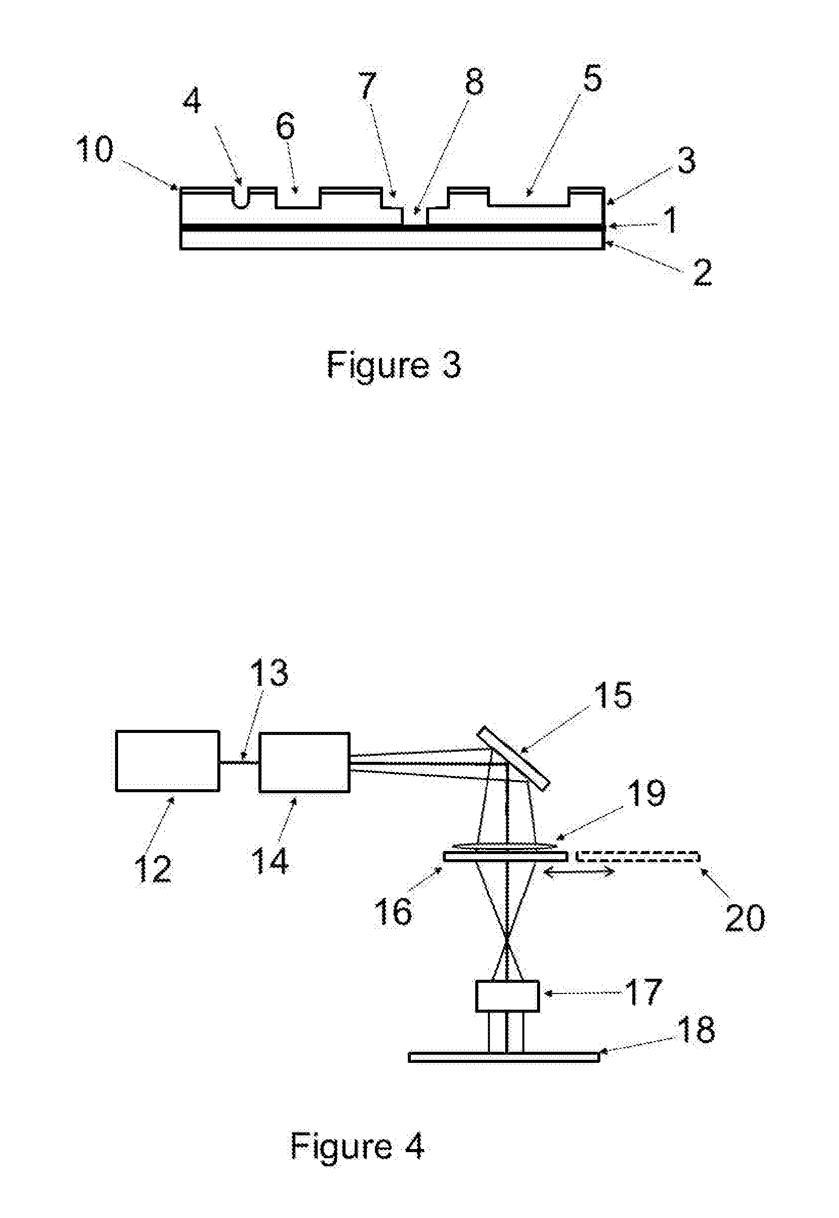
[0044]FIG. 1: This shows a section of a high density interconnect (HDI) printed circuit board (PCB) or integrated circuit (IC) substrate and indicates the type of “embedded” structures that are required to be formed. A copper layer 1, patterned to form an electrical circuit, is supported on a dielectric core layer 2. The copper layer 1 is over coated with an upper dielectric layer 3 into which various structures have been formed by laser ablation. Grooves 4, 4′ and 4″, large pad 5 and small pads 6 and 7 all have the same depth which is less than the full thickness of the upper dielectric layer 3. For IC substrates, groove widths and pad diameters required are typically in the range 5 to 15 microns and 100 to 300 μm, respectively, with depths in the range 5 to 10 microns. For HDI PCBs, grooves may be wider and deeper. Contact hole (or via) 8 inside pad 7 is formed by laser ablation to a greater depth such that all the upper dielectric layer material is removed to expose an area of th...


PUM

PropertyMeasurementUnit
energyaaaaaaaaaa
diametersaaaaaaaaaa
diametersaaaaaaaaaa

Abstract

Apparatus and methods for forming fine scale structures (4, 4′, 4″, 5, 6, 7, 8) in the surface of a dielectric substrate (3) to two or more depths are disclosed. In an example, the apparatus 25 comprises a first solid state laser (12) arranged to provide a first pulsed laser beam (13), a first mask (16) having a pattern for defining a first set of structures (4, 6, 7, 8) at a first depth, a projection lens (17) for forming a reduced size image of said pattern on the surface (3) of the substrate and a beam scanner arranged to scan said first pulsed laser beam (13) in a two-dimensional raster scan relative to the first pattern to form a first set of structures (4, 6, 7, 5) at a first depth in the substrate, wherein the first or a further solid state laser is arranged to form a second set of structures (8) at a second depth in the substrate (3).

Description

TECHNICAL FIELD[0001]This invention relates to an apparatus and method for forming fine scale structures in the surface of a dielectric substrate. In a preferred arrangement, it is particularly relevant to the sequential formation of narrow groove, large area pad and ground-plane structures in the top surface of a layer of a polymer and drilling contact holes or vias to a greater depth for the purpose manufacturing multi-layer, high density interconnection devices based on buried conductors.BACKGROUND ART[0002]Lasers are widely used in the manufacture of advanced printed circuit boards (PCBs). A particularly well known example is the drilling of blind contact holes, so called micro-vias, in multi-layer PCBs. In this case ultra violet (UV) solid state lasers are often used to drill through a top copper layer and an underlying dielectric layer to allow contact to be made to a lower copper layer. In some cases, the cost effectiveness of this process is improved by using two different l...

Claims


Application Information

Patent Timeline
Patent Type & Authority Applications(United States)
IPC IPC(8): H05K3/00H01S3/00B23K26/06H05K3/46B23K26/073H01S3/0941H01S3/11
CPCH05K3/0026H01S3/0941H01S3/0071H01S3/0057H01S3/11H05K2203/0557H05K3/0073B23K26/073B23K26/0648B23K26/0661H05K3/46H05K3/0035B23K26/0821B23K26/082B23K26/066B23K26/361B23K2103/50H01L21/67115B23K26/362B23K26/402
Inventor MILNE, DAVID CHARLESRUMSBY, PHILIP THOMASMYLES, DAVID THOMAS EDMUND
Owner M SOLV LTD
Why Eureka
Try Eureka