
Substrate processing apparatus

Active Publication Date: 2015-08-20
TOKYO ELECTRON LTD
View PDF3 Cites 3 Cited by
  • Summary
  • Abstract
  • Description
  • Claims
  • Application Information

AI Technical Summary

Benefits of technology

The patent text describes a vacuum processing apparatus that can perform multiple processes to a substrate in vacuum atmosphere using multiple process modules in sequence. The process modules are arranged such that each process can be performed by all or at least two process modules. The substrate can be quickly transferred through the transfer chamber to another process module if the first module cannot be used. This allows the processes to continue without stopping the operation of the apparatus. This reduces the waste of substrates and avoids interruption of the series of processes. Therefore, the number of wasted substrates can be reduced.

Problems solved by technology

In the device described in Japanese Patent Laid-open Publication No. 2003-060008, the number of the processing chambers which can be connected to the second transfer chamber is limited, so that it is difficult to connect standby processing chambers to the second transfer chamber.
Further, multiple transfer arms are provided within the second transfer chamber, but a substrate cannot be delivered within the second transfer chamber, and, thus, the substrate is transferred through the processing chambers.
WO2009 / 060540, a transfer route for a substrate becomes very complicated, so that the throughput is decreased.

Method used


Image

  • Substrate processing apparatus
  • Substrate processing apparatus
  • Substrate processing apparatus

Examples


Embodiment Construction

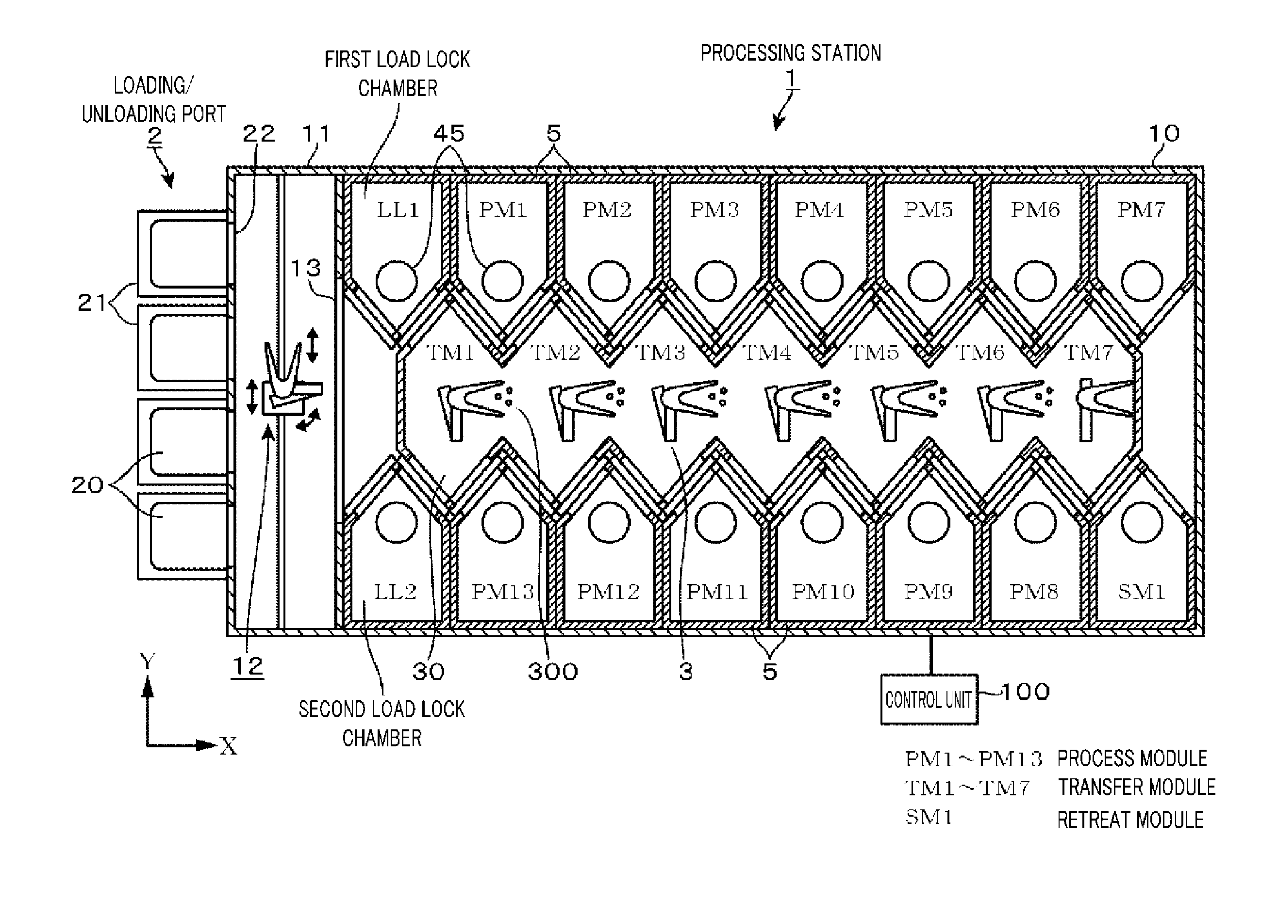
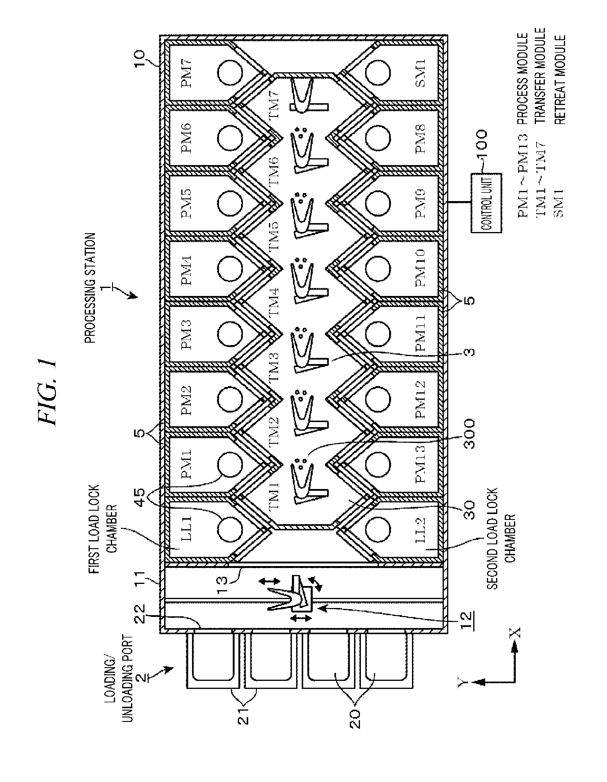
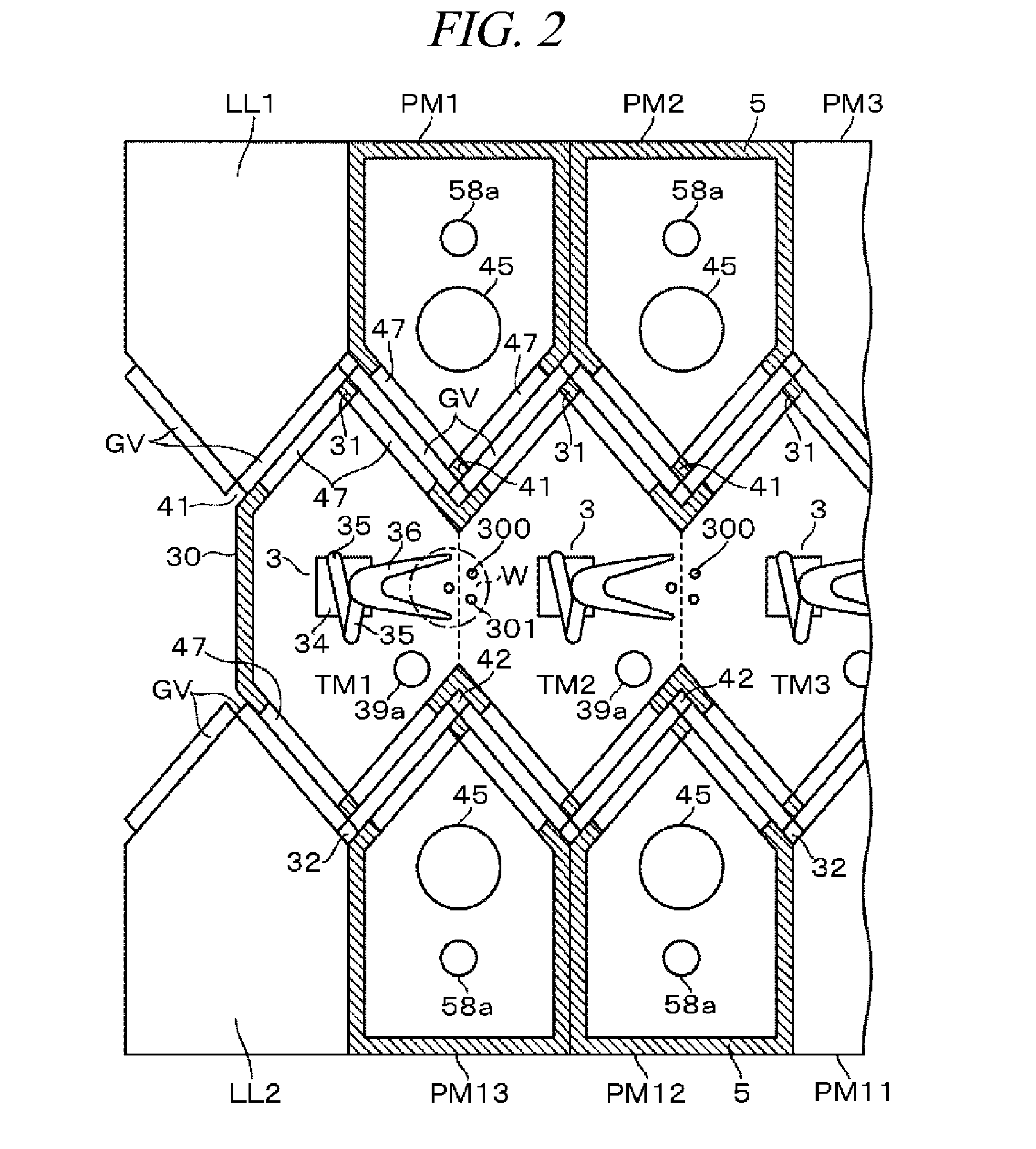
[0072]An example of a vacuum processing apparatus to which a substrate processing apparatus of an example embodiment is applied will be explained with reference to FIG. 1 to FIG. 18. This apparatus includes a processing station 1 arranged to be extended in an X direction (forward / backward direction) in FIG. 1 and configured to perform a process to a semiconductor wafer W (hereinafter, referred to as “wafer”) as a substrate in a vacuum atmosphere. An end of the processing station 1 is connected to a loading / unloading port 2 via an atmospheric transfer module 11. The loading / unloading port 2 is configured to load and unload the wafer W with respect to the processing station 1. In the loading / unloading port 2, a mounting table 21 serving as a loading port is arranged at multiple positions, for example, four positions, in a Y direction (right and left direction) in FIG. 1. On each mounting table 21, a FOUP 20 as a transfer container accommodating, for example, 25 wafers W is mounted. Re...


PUM

PropertyMeasurementUnit
Shapeaaaaaaaaaa

Abstract

An apparatus includes a row of substrate transfer devices 3 which can deliver a wafer W within a transfer chamber; and rows of process modules PM, arranged at right and left sides of the row of the substrate transfer devices along the row, configured to perform processes to the wafer W. The rows of the process modules PM are arranged such that each of the processes can be performed by at least two process modules PM. Thus, when a single process module PM cannot be used, the wafer W can be rapidly transferred to another process module PM which can perform the same process as performed in the corresponding process module. Therefore, even when the single process module PM cannot be used, the processes can be continued to the wafers W without stopping an operation of the apparatus, so that the number of wasted wafers W can be reduced.

Description

TECHNICAL FIELD[0001]The embodiments described herein pertain generally to a substrate processing apparatus that performs a series of processes to a substrate in a vacuum atmosphere using multiple process modules in sequence.BACKGROUND[0002]Recently, there has been a requirement for promoting non-volatilization of a system internal memory, and there has been suggested a MRAM (Magnetoresistive Random Access Memory) which uses a Tunneling Magnetoresistive (TMR) effect. The MRAM includes a MTJ (Magnetic Tunnel Junction) device at an intersection point between a word line and a bit line, and the MTJ device stores one-bit information. This MTJ device 9, as depicted in FIG. 58 and FIG. 59, serves as a laminated film in which a tunnel barrier layer is formed by interposing an insulating layer 96 between two ferromagnetic layers 95 (95a and 95b). In the MTJ device 9, when the magnetization directions of the two ferromagnetic layers 95 are identical with each other, electric resistance is lo...

Claims


Application Information

Patent Timeline
IPC IPC(8): H01J37/32
CPCH01L21/67173H01L21/6719H01L21/67196H01L21/67745C23C14/568H01J37/32899H01J37/32733H10N50/01C23C14/566H01L21/67161H01L21/67184
Inventor GOMI, ATSUSHIMIYASHITA, TETSUYAFURUKAWA, SHINJIMAEDA, KOJIHARA, MASAMICHISUZUKI, NAOYUKIMIKI, HIROSHIHIRATA, TOSHIHARU
Owner TOKYO ELECTRON LTD
Features
  • Generate Ideas
  • Intellectual Property
  • Life Sciences
  • Materials
  • Tech Scout
  • Unparalleled Data Quality
  • Higher Quality Content
  • 60% Fewer Hallucinations
Learn More