Multi-Layered Electronic System

a multi-layered electronic system and electronic system technology, applied in the direction of electrical equipment, coupling device connection, association of printed circuit non-printed electric components, etc., can solve the problem of great difficulty in providing adequate electrical connections between primary and security conductive tracks without external for

Active Publication Date: 2015-09-10
JOHNSON ELECTRIC SA
View PDF2 Cites 2 Cited by
  • Summary
  • Abstract
  • Description
  • Claims
  • Application Information

AI Technical Summary

Benefits of technology

[0019]Printed circuit boards offer an easily manufactured support for a primary conductive track, in addition to a flat surface onto which the flexible cover layer may be adhered. The printed circuit board is preferably rigid or substantially rigid, but it may also be a flexible substrate, as necessity dictates. A benefit therefore of the flexible cover layer is that the interposed layers are held in resilient permanent compression, irrespective of the rigidity of the mounting substrate.
[0021]To further enhance the physical and electrical connection between the security circuit, the conductive engagement element and the primary circuit, a spigot can be utilised. This advantageously applies a downward pressure onto the flexible cover layer, compressing the layers together towards the support substrate. This further prevents dislocation of the security layer, preventing accidental breakages of the security circuit and thus increasing device robustness and longevity.
[0024]A device being provided with a multi-layered electronic system allows for deactivation of the device when the security circuit is broken, in other words, when it is tampered with. This feature may be advantageous for a variety of devices. Furthermore, if the flexible cover layer is affixed to a housing of the electronic device, then dismantling the device will destroy the circuit, providing a further layer of protection against tampering.

Problems solved by technology

Up to now, there has been great difficulty in providing adequate electrical connections between the primary and security conductive tracks without the provision of an external force, for instance, that provided by a spigot.

Method used


Image

  • Multi-Layered Electronic System
  • Multi-Layered Electronic System
  • Multi-Layered Electronic System

Examples


first embodiment

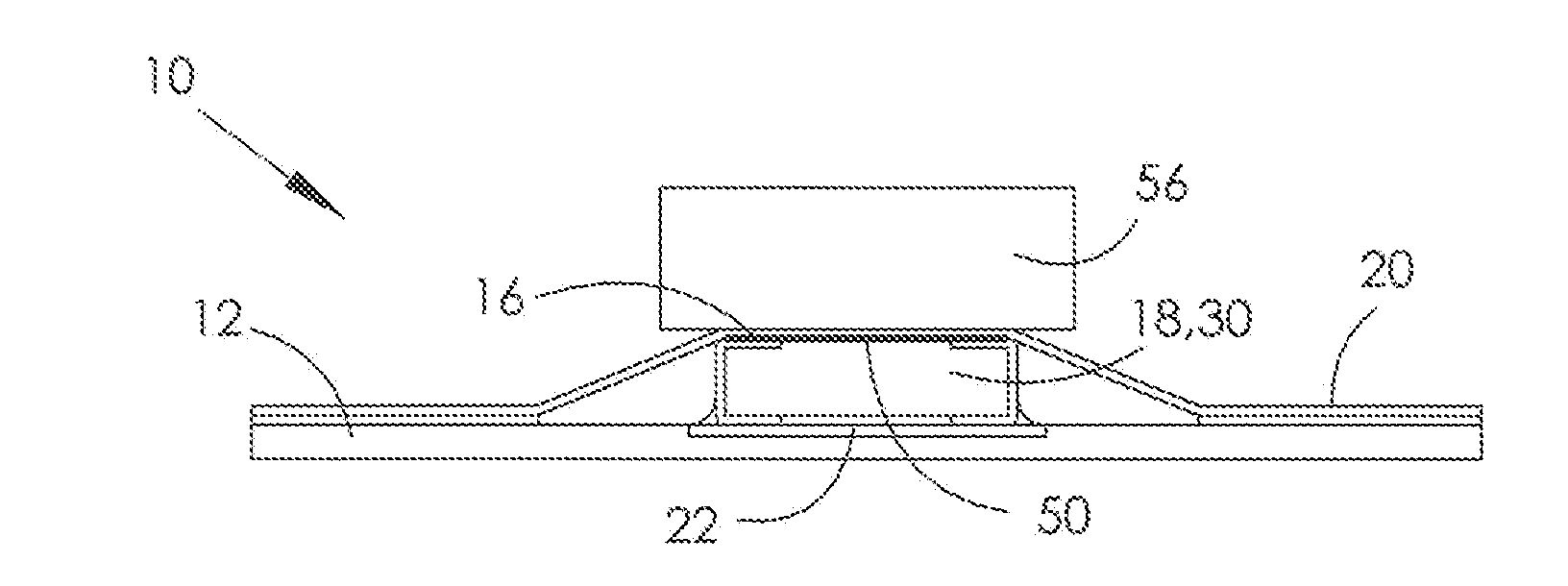
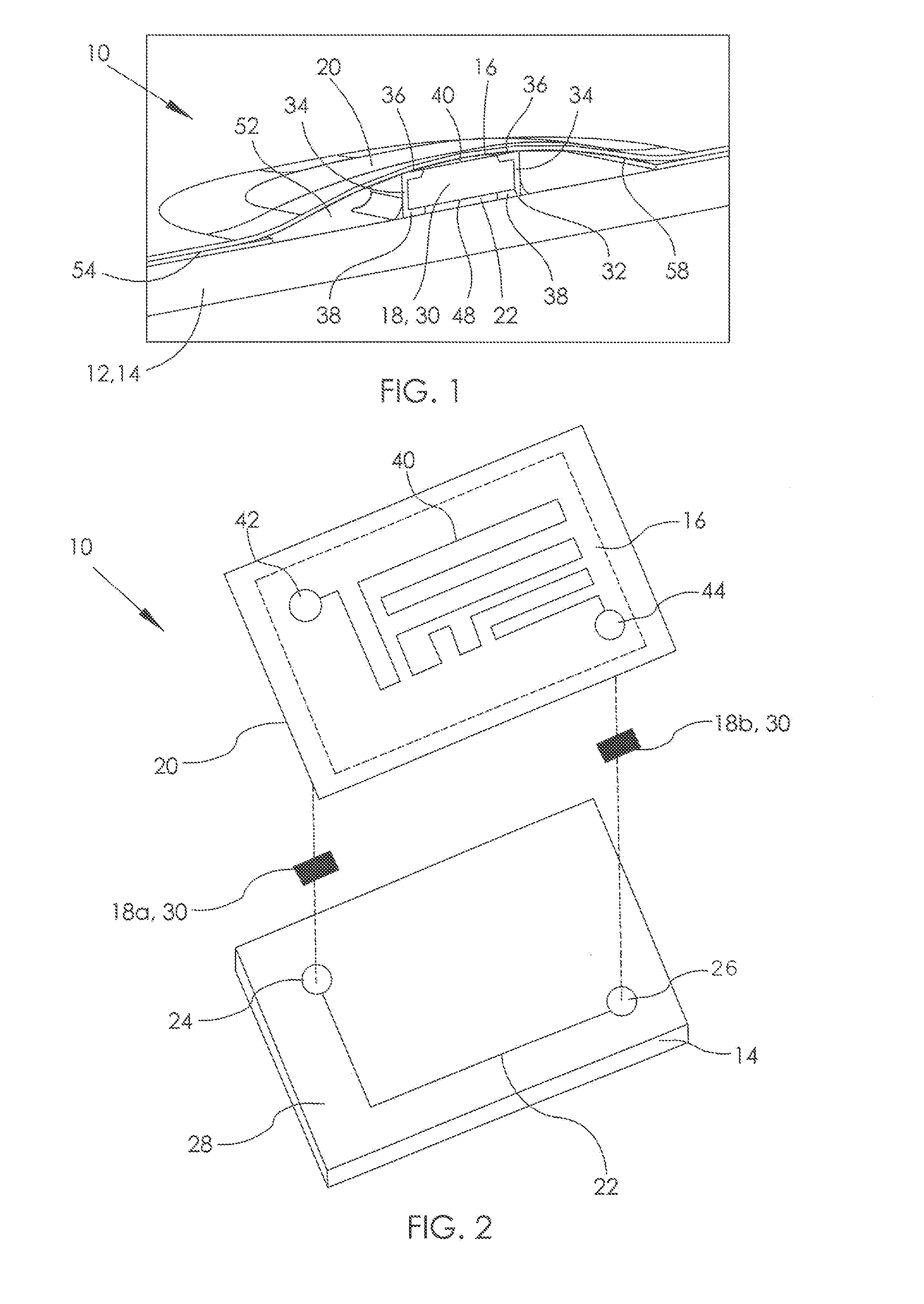
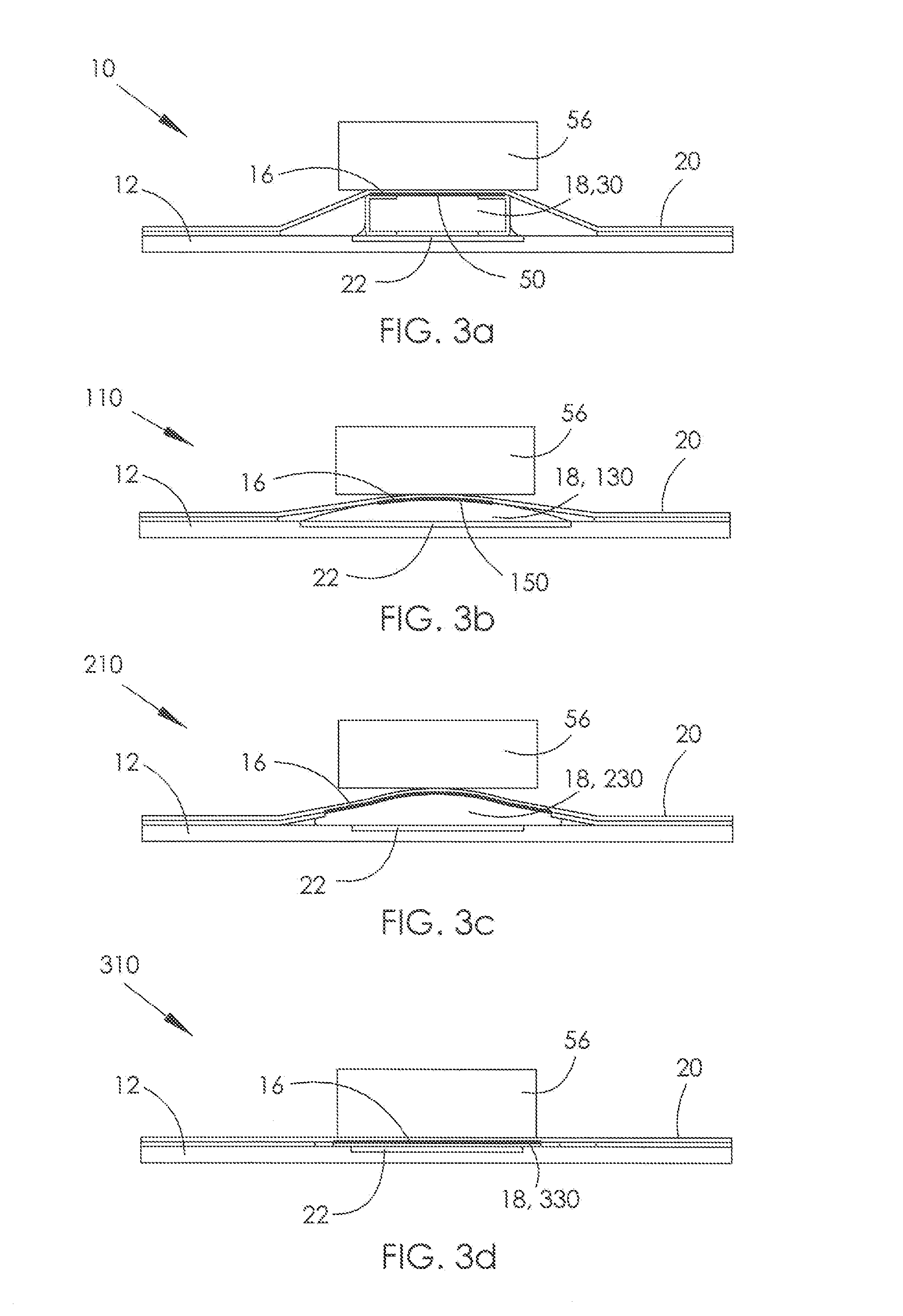
[0033]Referring firstly to FIGS. 1, 2 and 3a, there is shown a multi-layered electronic system 10 comprising a support substrate 12, in this case a printed circuit board (PCB) 14, a, preferably flexible, security layer 16, an electrically-conductive engagement element 18, and a flexible cover layer 20.

[0034]The PCB 14 includes at least one primary conductive track 22, basically represented for clarity in FIG. 2 by way of example only, the track 22 terminating at one end with a first primary terminal 24 and in a second primary terminal 26 at the opposing end. A first said electrically-conductive engagement element 18a is attached to the first primary terminal 24, and a further said electrically-conductive engagement element 18b is connected to the second primary terminal 26. The circuitry of the PCB 14 is the functional circuitry, and is referred to as the primary circuit 28.

[0035]In this first embodiment, each electrically-conductive engagement element 18a, 18b is a cuboidal resisto...

second embodiment

[0048]the electronic system 110 is shown in FIG. 3b, wherein the electrically-conductive engagement element 18 is provided as a solder bump 130 in lieu of a resistor 30. In this embodiment a piece of solder will be melted onto the primary conductive track 22 forming the solder bump 130, and a upper domed edge 150 of the bump 130 will contact with the security layer 16.

third embodiment

[0049]Alternatively, and as shown in FIG. 3c as the electronic system 210, the electrically-conductive engagement element 18 could be formed from an electrically-conductive foam 230 or other semi-rigid material. The foam 230 could be imbued with greater electrical conductivity by impregnating it with silver strands, for instance. It will be appreciated that whilst this particular embodiment discloses a deformable material as the electrically-conductive engagement element 18, it will still provide some tension to the flexible cover layer 20 to aid with retention of the security layer 16, and furthermore may be sticky or tacky to partially adhere the security layer 16 and / or flexible cover layer 20 to the foam 230.


PUM


Abstract

A multi-layered electronic system has a support substrate including at least a primary conductive track; a security layer including at least a conductive security track; an electrically-conductive engagement element in electrical communication with the primary conductive tack, and to which the security layer is mounted so that the conductive security track is in permanent electrical communication with the primary conductive track; and a flexible cover layer which overlies the security layer and which is directly or indirectly secured to the support substrate. The electrical connection between the security layer, conductive engagement element and primary conductive track is interrupted when the conductive security track is broken.

Description

CROSS REFERENCE TO RELATED APPLICATIONS[0001]This non-provisional patent application claims priority under 35 U.S.C. §119(a) from Patent Application No. GB1404188.3 filed in The United Kingdom on Mar. 10, 2014, the entire contents of which are hereby incorporated by reference.FIELD OF THE INVENTION[0002]The present invention relates to a multi-layered electronic system having a primary conductive track in permanent electrical connection with a conductive security track. The invention further relates to an anti-tamper electronic device utilising such a system, and to a method of deactivating such a device if tampered with.BACKGROUND OF THE INVENTION[0003]There are many electronic systems for which it is highly undesirable to permit tampering with the circuitry. For instance, any device relating to the security of financial transactions is vulnerable if the circuitry can be tampered with. A bank card reader, for example, could thus be backed or otherwise compromised to bypass the secu...

Claims


Application Information

Patent Timeline
Patent Type & Authority Applications(United States)
IPC IPC(8): H05K1/02H05K1/18
CPCH05K1/181H05K1/0275
Inventor MOREY, ALAN ROGEREDMONDS, MARTIN WALLACEKNIGHT, GREGORY TOBIASCOWCHER, ALEX JAMESHILSON, PAUL ALFREDSMITH, STEVEN MARK
Owner JOHNSON ELECTRIC SA
Why Eureka
Try Eureka