Thin film transistor array panel and manufacturing method thereof

a technology of thin film transistors and array panels, applied in transistors, electrical devices, semiconductor devices, etc., can solve the problems of reduced mobility of carriers, difficult realization of driving circuits operable at a relatively high rate, and uneven threshold voltages, etc., to achieve the effect of simple manufacturing process

Inactive Publication Date: 2015-09-24
SAMSUNG DISPLAY CO LTD
View PDF24 Cites 15 Cited by
  • Summary
  • Abstract
  • Description
  • Claims
  • Application Information

AI Technical Summary

Benefits of technology

[0020]According to one or more exemplary embodiment of the thin film transistor and the manufacturing method thereof of the invention, the threshold voltage (Vth) can be controlled to be uniform by red

Problems solved by technology

When the active layer includes amorphous silicon, mobility of carriers is reduced and realizing a driving circuit operable at a relatively high rate may be difficult.
When th

Method used


Image

  • Thin film transistor array panel and manufacturing method thereof
  • Thin film transistor array panel and manufacturing method thereof
  • Thin film transistor array panel and manufacturing method thereof

Examples


Embodiment Construction

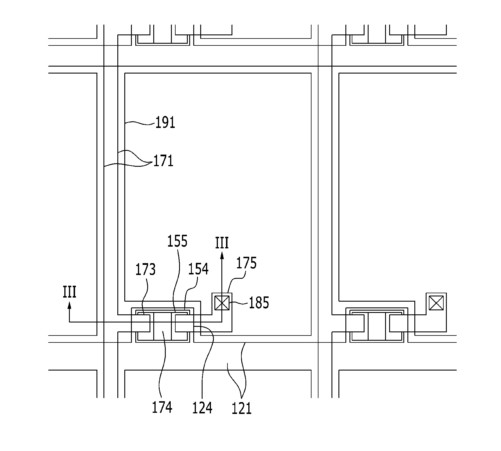
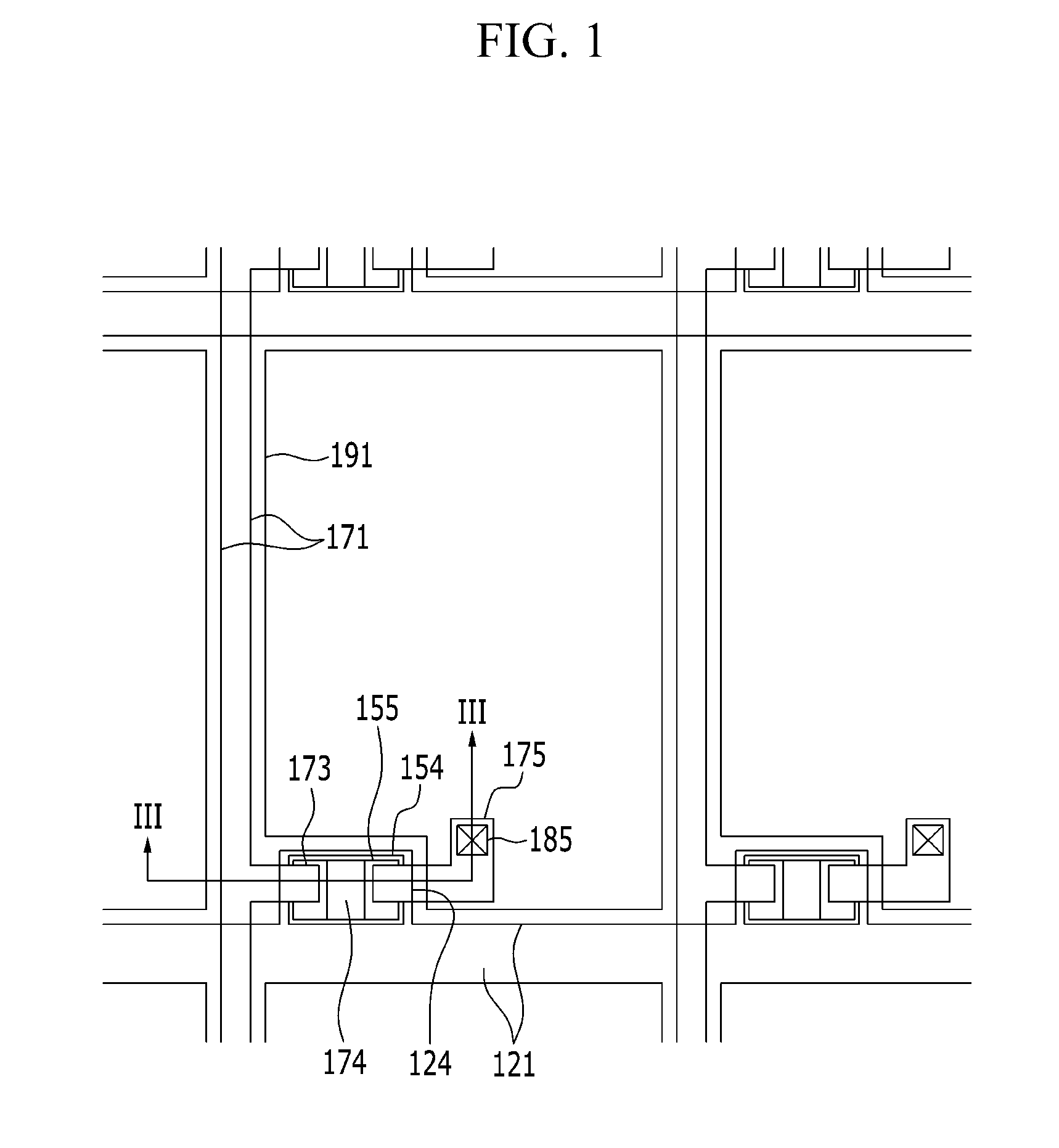
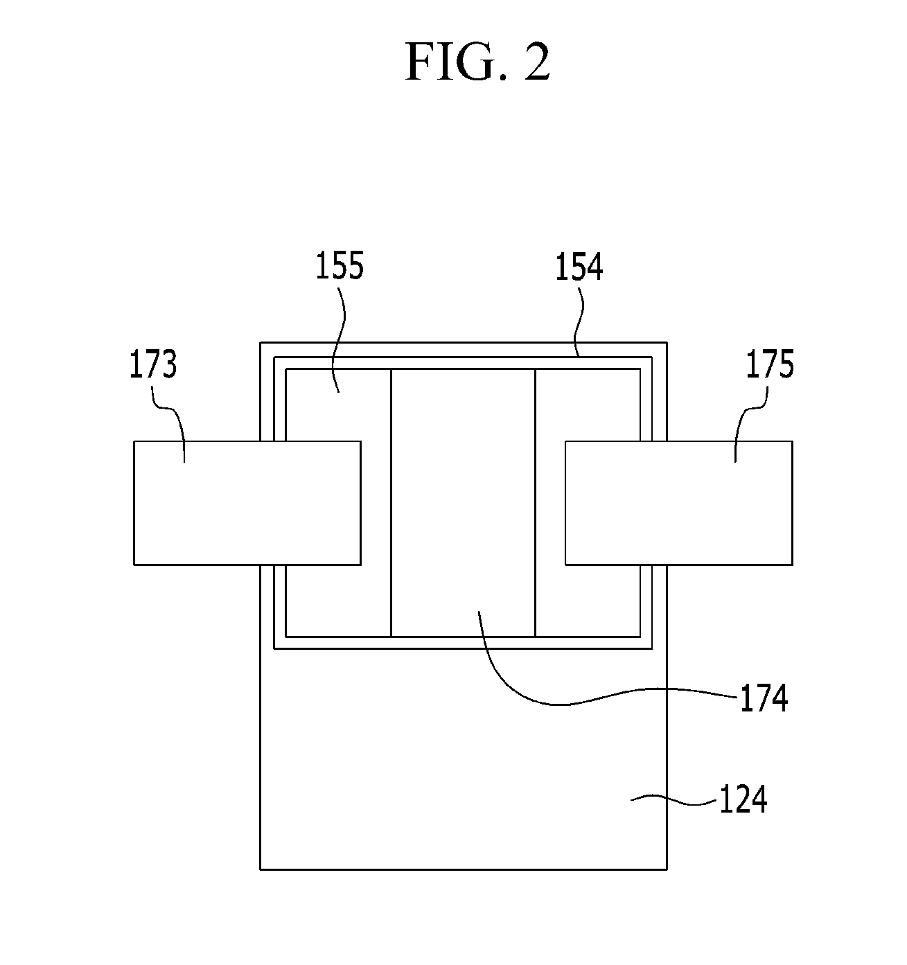
[0029]The invention will be described more fully hereinafter with reference to the accompanying drawings, in which exemplary embodiments of the invention are shown. As those skilled in the art would realize, the described embodiments may be modified in various different ways, all without departing from the spirit or scope of the invention.

[0030]In the drawings, the thickness of layers, films, panels, regions, etc., are exaggerated for clarity. Like reference numerals designate like elements throughout the specification. It will be understood that when an element such as a layer, film, region, or substrate is referred to as being “on” or “connected to” another element, it can be directly on or connected to the other element or intervening elements may also be present. In contrast, when an element is referred to as being “directly on” or “directly connected to” another element, there are no intervening elements present. As used herein, connected may refer to elements being physically ...


PUM


Abstract

A thin film transistor array panel includes: a substrate; a first gate electrode on the substrate; a gate insulating layer on the gate electrode; a semiconductor on the gate insulating layer; an etch stopper on a channel of the semiconductor; a source electrode and a drain electrode on the semiconductor and facing each other with respect to the first gate electrode; and a second gate electrode on the channel of the semiconductor and in a same layer as the source electrode and the drain electrode. The second gate electrode is electrically separated from the source electrode and the drain electrode.

Description

[0001]This application claims priority to Korean Patent Application No. 10-2014-0031848 filed on Mar. 18, 2014, and all the benefits accruing therefrom under 35 U.S.C. §119, the entire contents of which are incorporated herein by reference.BACKGROUND[0002](a) Field[0003]The invention relates to a thin film transistor array panel and a manufacturing method thereof, and particularly, the invention relates to a thin film transistor array panel including an etch stopper and a double gate electrode, and a manufacturing method thereof.[0004](b) Description of the Related Art[0005]A thin film transistor (“TFT”) such as a liquid crystal display element, an organic electroluminescent display element and an inorganic electroluminescent display element, used for a flat panel display, is used as a switching element for controlling respective pixels and a driving element for driving the pixels.[0006]In general, the TFT includes an active layer including source and drain regions doped with a rela...

Claims


Application Information

Patent Timeline
IPC IPC(8): H01L29/786H01L29/45H01L29/49H01L29/66
CPCH01L29/78648H01L29/66765H01L29/78672H01L29/7869H01L29/495H01L29/458H01L29/45H01L29/4908H01L29/66969
Inventor SONG, JUN HO
Owner SAMSUNG DISPLAY CO LTD
Why Eureka
Try Eureka