Reduction of light induced degradation in thin film silicon solar cells

a thin film silicon and solar cell technology, applied in the direction of sustainable manufacturing/processing, climate sustainability, semiconductor devices, etc., can solve the problems of negatively affecting the quantity of solar cells, reducing the efficiency of solar cells, etc., to reduce the degradation of photovoltaic devices, reduce the offset of bands, and reduce the effect of light-induced degradation of devices

Inactive Publication Date: 2015-09-24
IBM CORP +1
View PDF19 Cites 1 Cited by
  • Summary
  • Abstract
  • Description
  • Claims
  • Application Information

AI Technical Summary

Benefits of technology

[0011]A device and method for reducing degradation in a photovoltaic device includes adjusting a band offset of the device during one or more of forming an electrode, forming a first doped layer or forming an intrinsic layer. The adjusting reduces a band offset between one or more of the electrode, the first doped layer and the intrinsic layer to reduce light-induced degradation of the device. A second doped layer is formed on the intrinsic layer.
[0012]A method for reducing degradation in a photovoltaic device includes forming a bi-layer electrode by providing different dopant concentrations of the bi-layer electrode relative to a first doped layer to be formed thereon such that the bi-layer has a lower dopant concentration in contact with the first doped layer than other portions of the bi-layer electrode to reduce band offset between the bi-layer electrode and the first doped layer; forming the first doped layer and an intrinsic layer on the first doped layer while adjusting a band offset between layers by adjusting dopant types and concentrations in at least one of the first doped layer and the intrinsic layer, such that light induced degradation is reduced with lower band offset between one or more of the bi-layer electrode, the first doped layer and the intrinsic layer; and forming a second doped layer.

Problems solved by technology

The solar cell experiences reduced fill factor (FF) and reduced open circuit voltage (Voc) both of which reduce the efficiency of the solar device.
These quantities are negatively affected in solar cells by light induced cell degradation.

Method used


Image

  • Reduction of light induced degradation in thin film silicon solar cells
  • Reduction of light induced degradation in thin film silicon solar cells
  • Reduction of light induced degradation in thin film silicon solar cells

Examples


Embodiment Construction

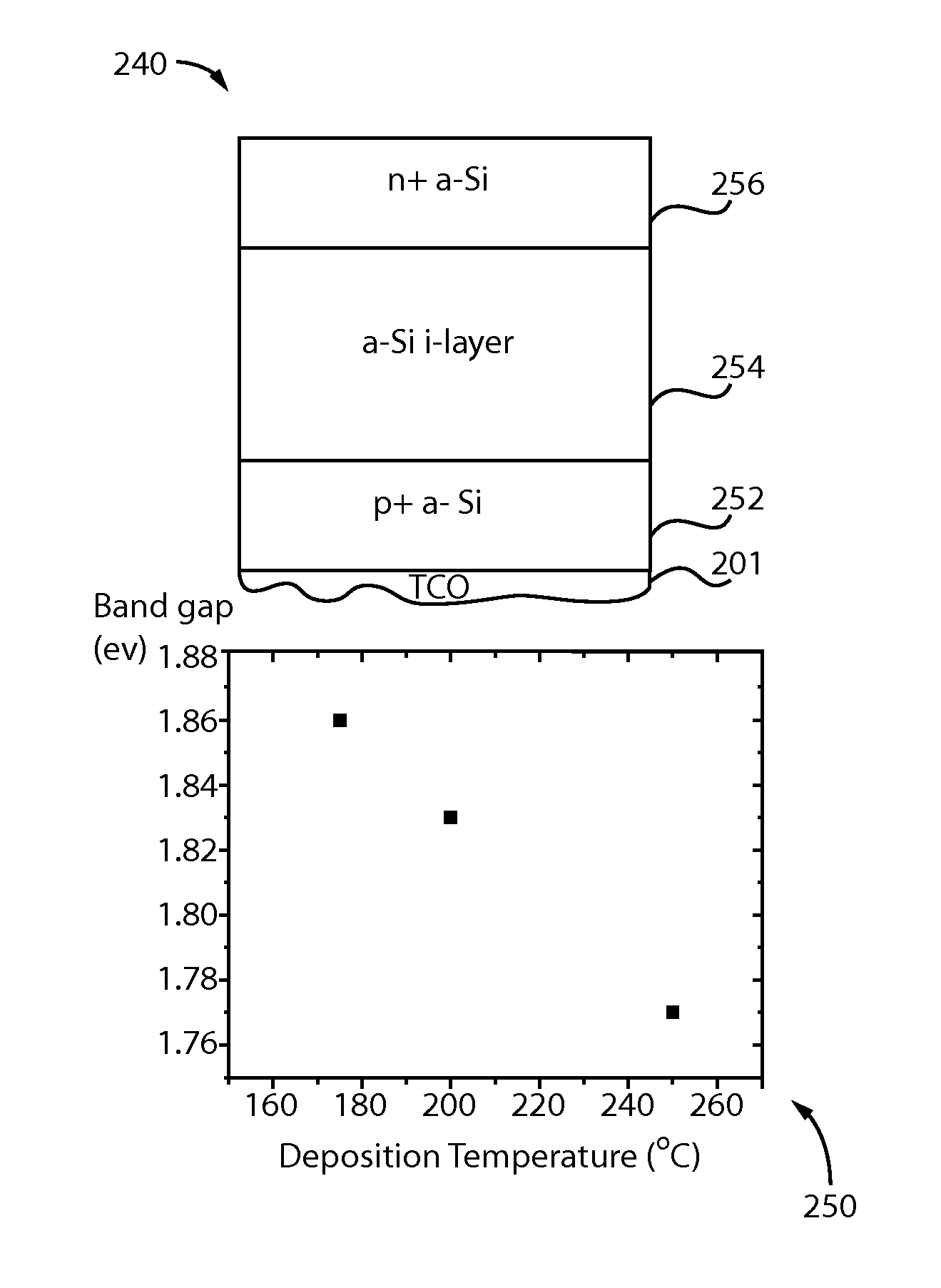
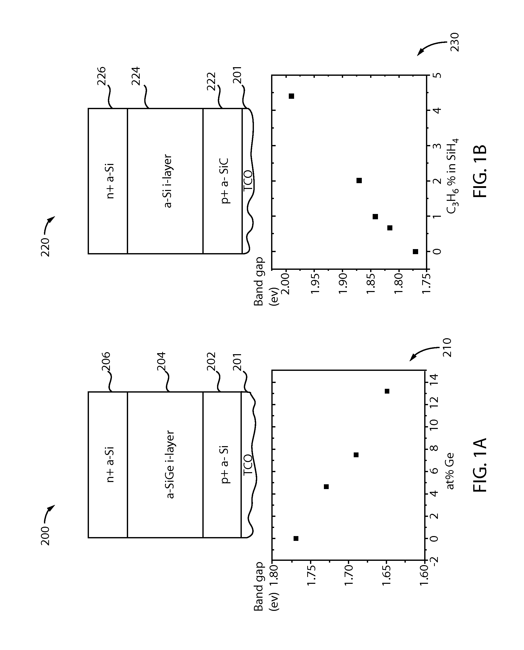
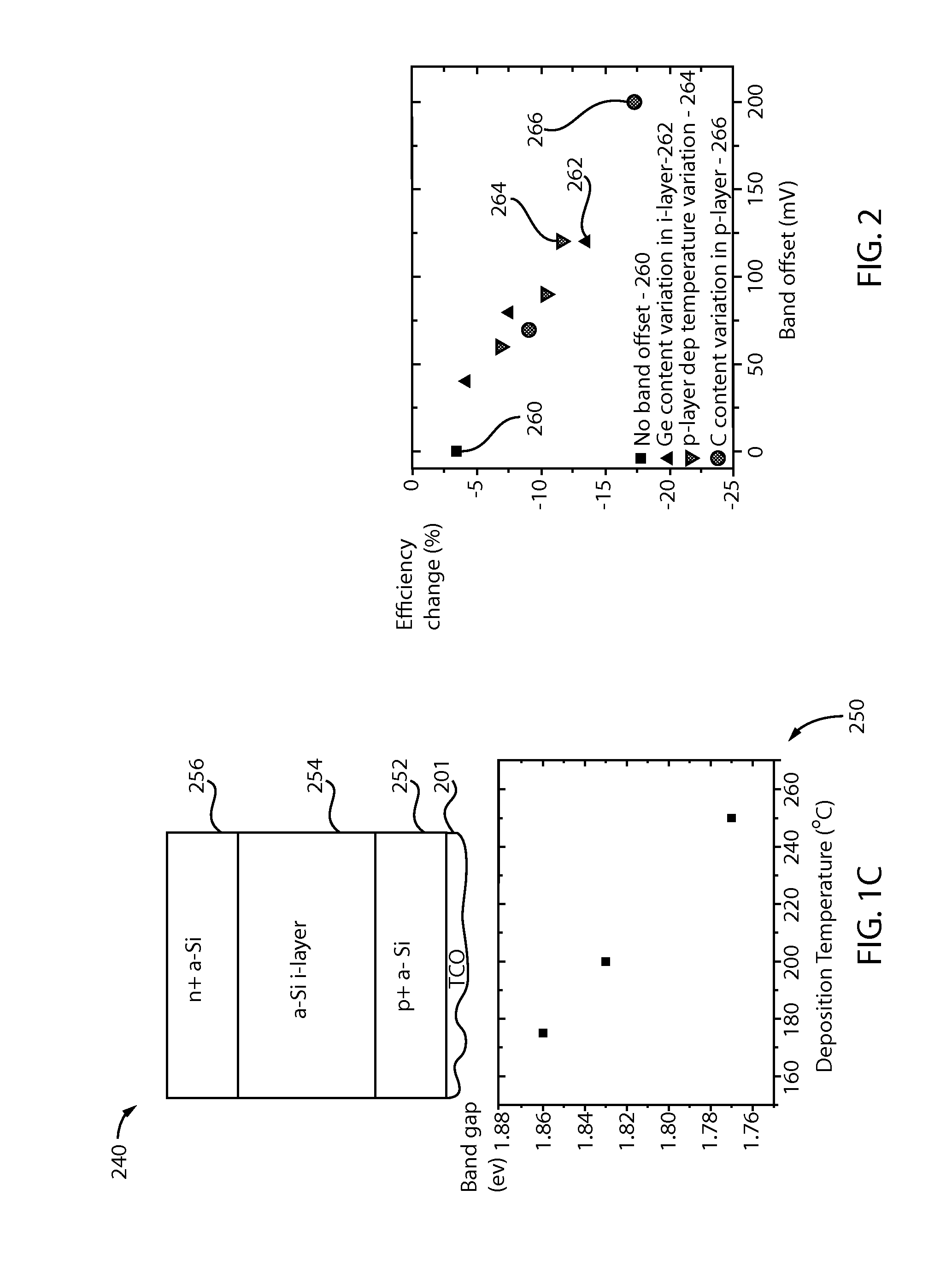
[0024]In accordance with the present principles, methods and devices are presented that provide light induced degradation resistance. Light induced degradation occurs in a semiconductor structure when the structure becomes saturated by incoming radiation (light soaked). The structure begins to degrade due in part to the reconfiguration of hydrogen atoms, which results in passivation and bond breaking between constituent materials. This degradation process becomes prominent if there exists a band offset at a p-i interface and / or at a transparent conductive oxide (TCO) to p+ interface—as discovered by the present inventors. This new mechanism is addressed in view of the Staebler-Wronski effect (SW effect) to provide improved solar devices. Based on this understanding, strategies for minimizing the SW effect are introduced.

[0025]Band offset at the p-i interface cannot be avoided since high band gap materials are required for the p+ layer whereas low band gap materials are desirable for...


PUM


Abstract

A device and method for reducing degradation in a photovoltaic device includes adjusting a band offset of the device during one or more of forming an electrode, forming a first doped layer or forming an intrinsic layer. The adjusting reduces a band offset between one or more of the electrode, the first doped layer and the intrinsic layer to reduce light-induced degradation of the device. A second doped layer is formed on the intrinsic layer.

Description

RELATED APPLICATION INFORMATION[0001]This application is a Divisional application of copending U.S. patent application Ser. No. 13 / 185,860, filed on Jul. 19, 2011, which is incorporated herein by reference in its entirety.BACKGROUND[0002]1. Technical Field[0003]The present invention relates to photovoltaic devices and methods for fabrication, and more particularly to devices, structures and fabrication methods that reduce light-induced degradation by material selection and by adjusting band offsets.[0004]2. Description of the Related Art[0005]Solar devices employ photovoltaic cells to generate current flow. Photons in sunlight hit a solar cell or panel and are absorbed by semiconducting materials, such as silicon. Carriers gain energy allowing them to flow through the material to produce electricity. The solar cell converts the solar energy into a usable amount of electricity.[0006]When a photon hits a piece of silicon, the photon may be transmitted through the silicon, the photon c...

Claims


Application Information

Patent Timeline
Patent Type & Authority Applications(United States)
IPC IPC(8): H01L31/075H01L31/0376H01L31/0224
CPCH01L31/075H01L31/03767H01L31/022475H01L31/022483H01L31/202H01L31/204Y02E10/548Y02P70/50
Inventor ABOU-KANDIL, AHMEDHONG, AUGUSTIN J.KIM, JEEHWANSAAD, MOHAMEDSADANA, DEVENDRA K.
Owner IBM CORP
Why Eureka
Try Eureka