
Substrate having concave-convex pattern, light-emitting diode including the substrate, and method for fabricating the diode

a technology of concave convex pattern and substrate, applied in the field of semiconductor devices, can solve problems such as crystal defects in the epitaxial semiconductor layer

Active Publication Date: 2015-09-24
SEOUL VIOSYS CO LTD
View PDF34 Cites 4 Cited by
  • Summary
  • Abstract
  • Description
  • Claims
  • Application Information

AI Technical Summary

Benefits of technology

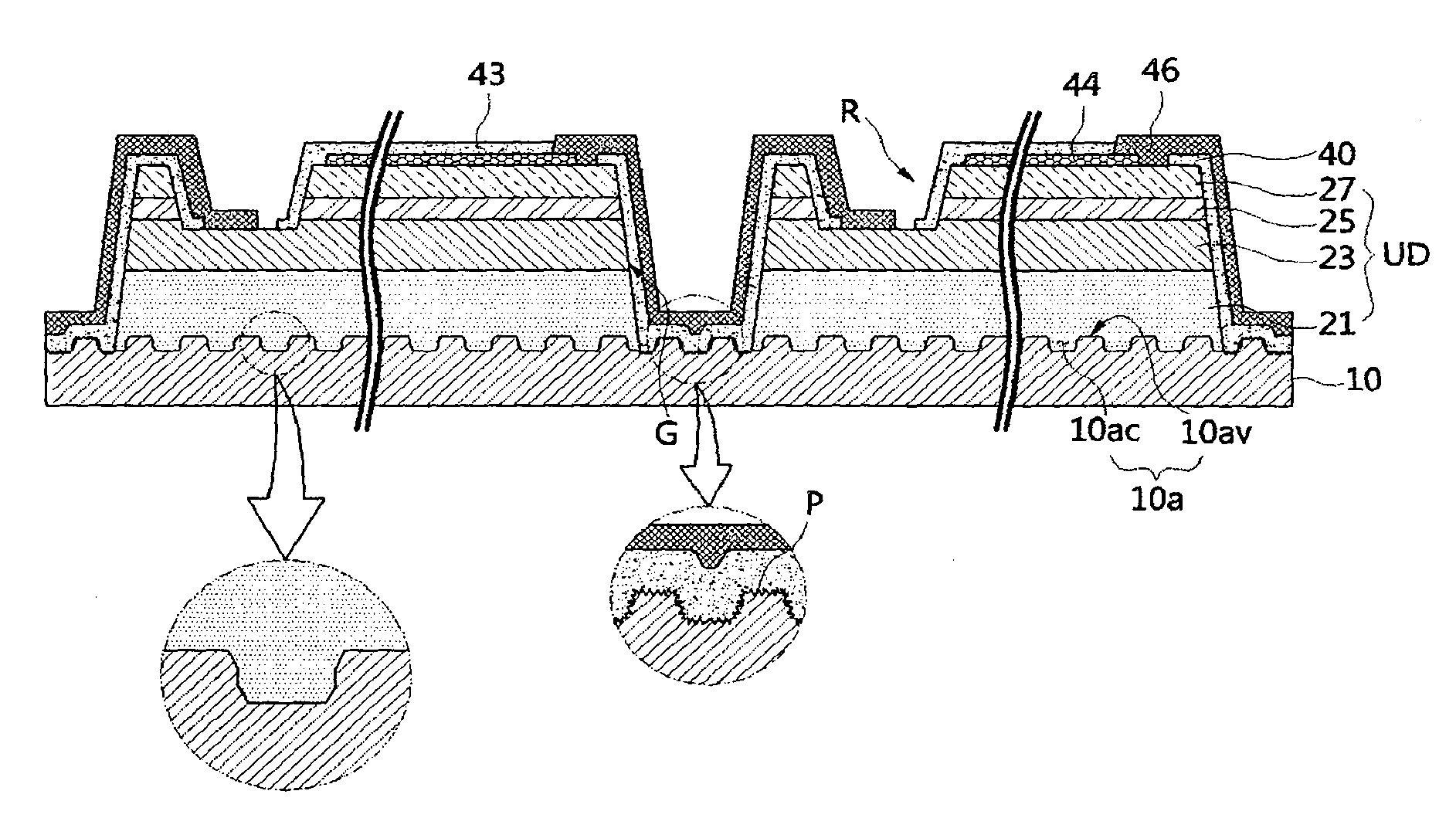
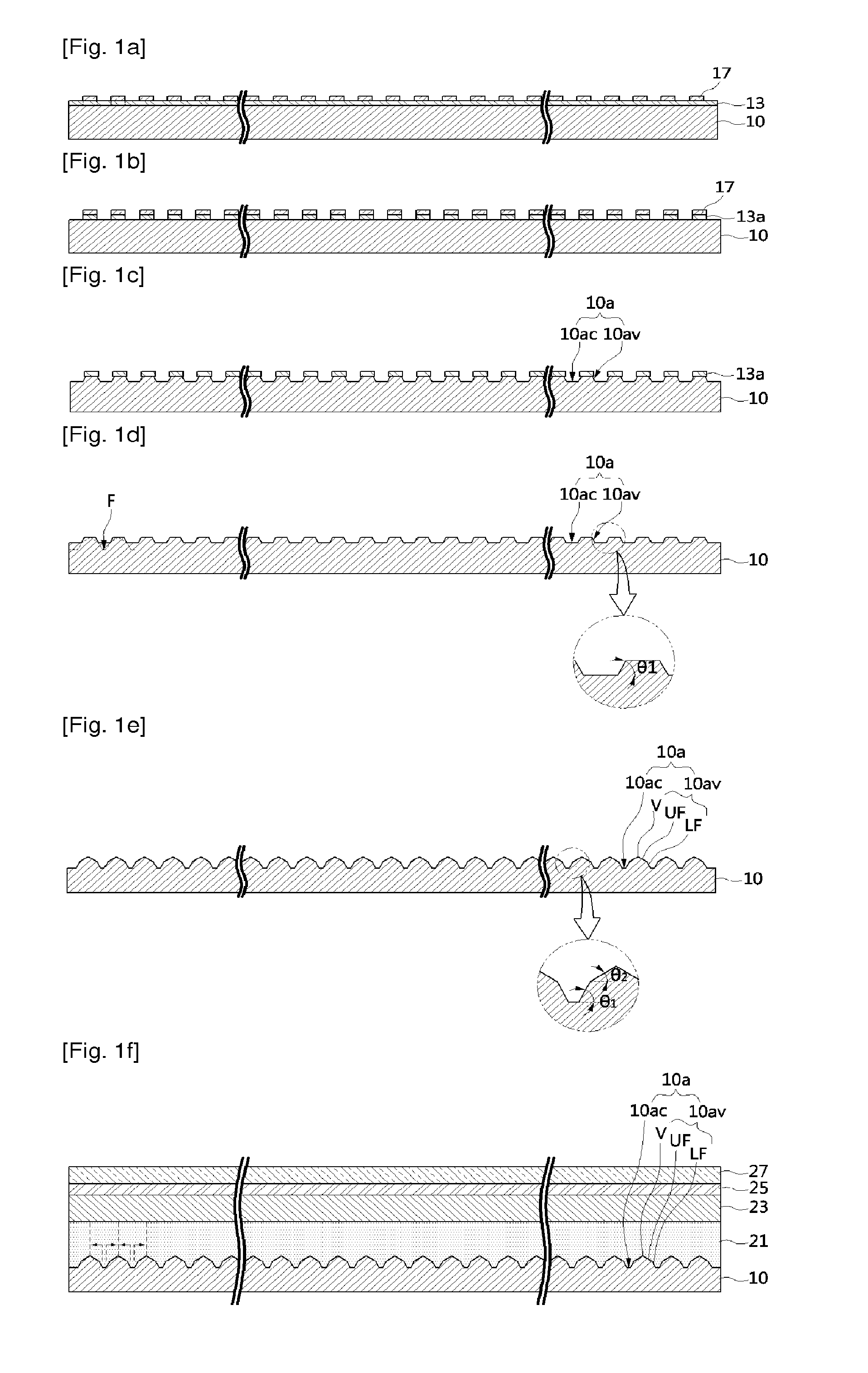
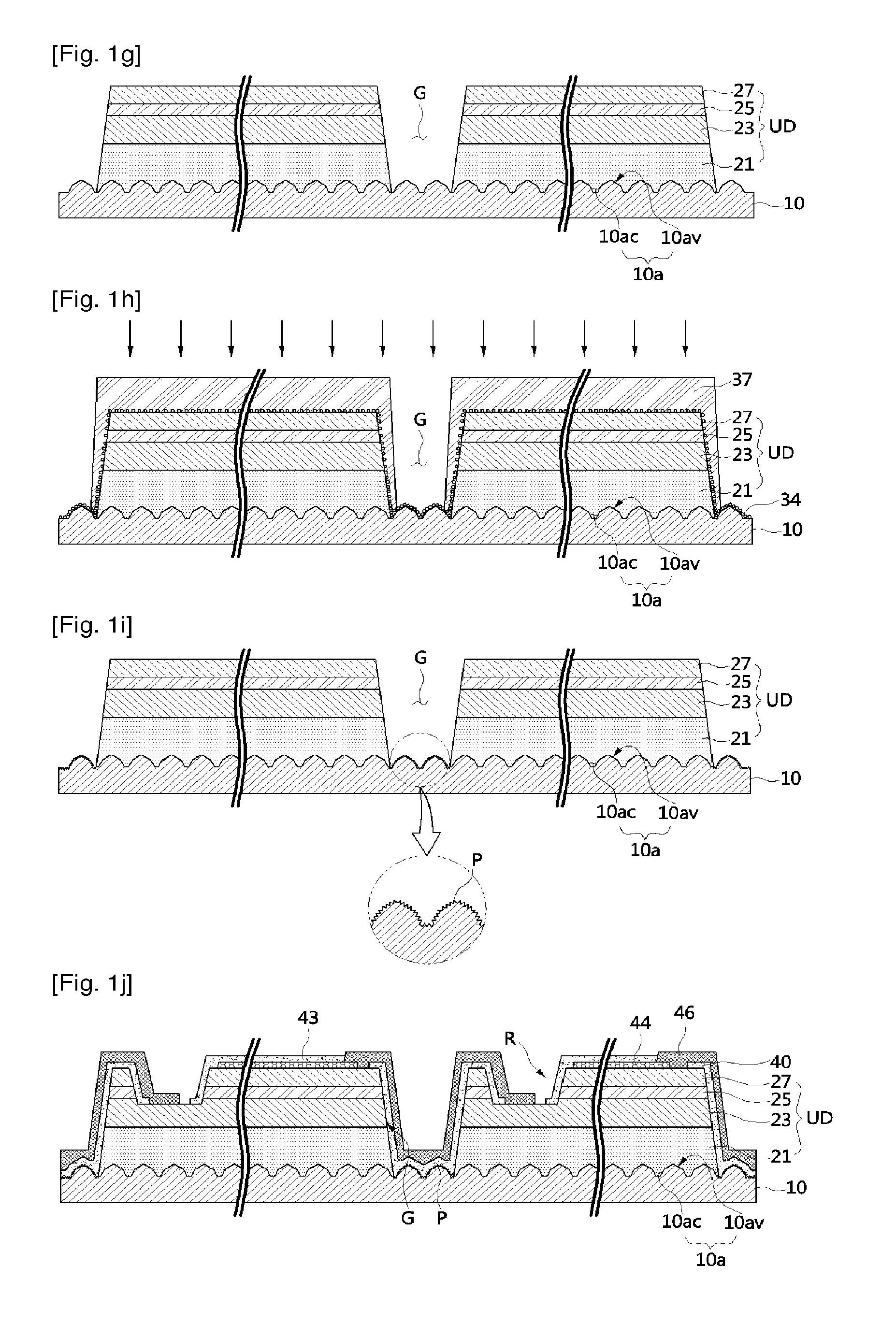
The present invention provides an LED with improved light extraction efficiency and reduced crystal defects. This is achieved by creating concave-convex patterns on the LED and stabilizing the facets through crystallography. This improves the quality of the epitaxial layer formed on the concave-con convex patterns.

Problems solved by technology

However, such concave-convex patterns may cause crystal defects in the epitaxial semiconductor layer.

Method used


Image

  • Substrate having concave-convex pattern, light-emitting diode including the substrate, and method for fabricating the diode
  • Substrate having concave-convex pattern, light-emitting diode including the substrate, and method for fabricating the diode
  • Substrate having concave-convex pattern, light-emitting diode including the substrate, and method for fabricating the diode

Examples


fabrication example 3

of LED

[0118]An LED was fabricated using a similar method to that of LED fabrication example 1 except that a substrate according to concave-convex fabrication example 3 was used.

[0119]FIG. 14 and FIG. 15 are scanning electron microscope (SEM) images respectively taken after epitaxial layers were grown on concave-convex patterns in accordance with concave-convex pattern fabrication examples 1 and 2.

[0120]Referring to FIG. 14 and FIG. 15, when a concave-convex pattern was formed by dry etching, crystallographic mismatch such as a fine void VD generated between an inclined plane of the concave-convex pattern and an epitaxial layer 121, and also dislocation D occurred in the epitaxial layer 121 (LED fabrication example 2, FIG. 15). On the other hand, when a concave-convex pattern 10a was formed by wet etching, no fine void VD was observed on the interface between an inclined plane of the concave-convex pattern 10a and an epitaxial layer 21, almost no dislocation was observed, and thus it...


PUM


Abstract

Provided are a substrate having concave-convex patterns, a light-emitting diode (LED) including the substrate, and a method of fabricating the LED. The LED includes a substrate, and concave-convex patterns disposed in an upper surface of the substrate and having convexes and concaves defined by the convexes. Unit light-emitting device having a first conductive semiconduct or layer, an active layer, and a second conductive semiconductor layer disposed on the substrate in sequence is present.

Description

CROSS-REFERENCE TO RELATED APPLICATIONS[0001]This application is the National Stage Entry of International Application PCT / KR2012 / 007912, filed on Sep. 28, 2012, and claims priority from and the benefit of Korean Patent Application No. 10-2011-0100097, filed on Sep. 30, 2011, which are incorporated herein by reference for all purposes as if fully set forth herein.BACKGROUND[0002]1. Field[0003]The present invention relates to a semiconductor device, and more particularly, to a light-emitting diode (LED).[0004]2. Discussion of the Background[0005]An LED is a device having an n-type semiconductor layer, a p-type semiconductor layer, and an active layer disposed between the n-type and p-type semiconductor layers. When a forward electric field is applied to the n-type and p-type semiconductor layers, electrons and holes are injected into the active layer, and the injected electrons and holes are recombined in the active layer to emit light.[0006]The efficiency of such an LED is determine...

Claims


Application Information

Patent Timeline
Patent Type & Authority Applications(United States)
IPC IPC(8): H01L33/20H01L33/16H01L33/32H01L27/15H01L33/06H01L33/14
CPCH01L33/20H01L33/06H01L33/16H01L33/32H01L27/153H01L33/14H01L33/007H01L33/10H01L33/22
Inventor KIM, JAE KWONLEE, SUM GEUNKIM, KYUNG WANYOON, YEO JINSUH, DUK ILKIM, JI HYE
Owner SEOUL VIOSYS CO LTD
Learn More