Semiconductor substrate and process for production thereof

a technology of semiconductor substrate and semiconductor, applied in the direction of semiconductor/solid-state device manufacturing, basic electric elements, electric apparatus, etc., can solve the problems of mbe and lpvpe, suitable for fipos structure production, and coarse porous structure,

Inactive Publication Date: 2000-10-24
CANON KK
View PDF13 Cites 32 Cited by
  • Summary
  • Abstract
  • Description
  • Claims
  • Application Information

AI Technical Summary

Problems solved by technology

However, such a high-temperature treatment causes considerable coarsening of porous structure, which is not suitable for production of the FIPOS structure.
The studies on the FIPOS process were actively conducted from 1970s to the first half of 1980s, but have declined with development of new processes for SOI structures because the formation of the surface silicon layer is limited to island shapes in the FIPOS process, which is not suitable for general purposes.
Therefore, the epitaxial growth method has been limited to MBE and LPVPE which have not widely been used for semiconductor silicon production.
The pin holes would cause leakage, or poor dielectric strength.
In this Lasky's method, it is difficult to leave the epitaxial silicon layer in a uniform thickness on the entire face of the wafer since the ratio of the etching rate of p' silicon to that of the epitaxial (p- or n) silicon is low.
Therefore, the heat treatment after the lamination must be conducted at the temperature not higher than 800.degree. C., and further the repeated etching is expected to be not satisfactorily controlled in mass production owing to low selectivity ratio in respective etching steps.
Generally, the lamination defects are considered to possibly deteriorate the dielectric strength of the oxide layer.
This may cause etching of the buried silicon oxide to form voids.
In the resulting void portion, where no buried oxide film is present, failure of a device like a MOS transistor may result owing to instability of the underlying interface.
If the epitaxial layer is laminated directly to the supporting substrate in the subsequent step, impurities are liable to segregate at the lamination interface, and dangling bonds of the atoms at the interface tends to increase to render unstable the properties of the resulting thin film device.
However, an excessively high temperature can cause structural change of the porous layer 101, or diffusion of an impurity from the substrate to the epitaxial layer.
Some substrates are not capable of enduring heat treatment at a high temperature.
However, the oxidation should be limited to be at the surface of the inner walls of the pores to keep the monocrystallinity in the interior of t...

Method used


Image

  • Semiconductor substrate and process for production thereof
  • Semiconductor substrate and process for production thereof
  • Semiconductor substrate and process for production thereof

Examples


example 2

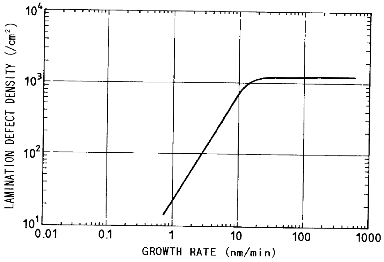
This Example shows reduction of crystal defects in an epitaxial silicon layer formed on a porous silicon without decreasing the growth rate.

(1) Five 5-inch silicon(100) wafers were prepared which contained boron as a p-type impurity, and had a resistivity of 0.01 to 0.02 .OMEGA.cm.

(2) In a mixed solution composed of 49% HF and ethyl alcohol (mixing ratio 2:1), the above silicon wafer was placed as the anode, and a platinum plate of 5 inch diameter was placed as the cathode in opposition to the silicon wafer. The back face of the silicon wafer was coated to prevent conduction to the platinum plate through the solution. The side edge of the silicon wafer was also coated, whereas the entire of the front face of the silicon wafer was bared to conduct to the platinum plate through the solution. The silicon wafer was anodized by applying electric current between the silicon wafer and the platinum plate at a current density of 10 mA / cm.sup.2 for 12 minutes to form a porous silicon surfac...

example 3

(1) Five 5-inch silicon (100) wafers were prepared which contained boron as a p-type impurity, and had a resistivity of 0.01 to 0.02 .OMEGA.cm.

(2) In a mixed solution composed of 49% HF and ethyl alcohol (mixing ratio 2:1), the above silicon wafer was placed as the anode, and a platinum plate of 5 inch diameter was placed as the cathode in opposition to the silicon wafer. The reverse face of the silicon wafer was coated to prevent conduction to the platinum plate through the solution. The side edge of the silicon wafer was also coated, whereas the entire of the front face of the silicon wafer was bared to conduct to the platinum plate through the solution. The silicon wafer was anodized by applying electric current between the silicon wafer and the platinum plate at a current density of 10 mA / cm.sup.2 for 12 minutes to form a porous silicon surface layer of 12 .mu.m thick. This anodization was practiced for respective wafers separately. One of the wafers having a porous layer was ...

example 4

(1) Five 5-inch silicon (100) wafers were prepared which contained boron as a p-type impurity, and had a resistivity of 0.01 to 0.02 .OMEGA.cm.

(2) In a mixed solution composed of 49% HF and ethyl alcohol (mixing ratio 2:1), the above silicon wafer was placed as the anode, and a platinum plate of 5 inch diameter was placed as the cathode in opposition to the silicon wafer. The reverse face of the silicon wafer was coated to prevent conduction to the platinum plate through the solution. The side edge of the silicon wafer was also coated, whereas the entire of the front face of the silicon wafer was bared to conduct to the platinum plate through the solution. The silicon wafer was anodized by applying electric current between the silicon wafer and the platinum plate at a current density of 10 mA / cm.sup.2 for 12 minutes to form a porous silicon surface layer 12 .mu.m thick. This anodization was practiced for respective wafers separately. One of the wafers having a porous layer was sub...


PUM


Abstract

A process for producing a semiconductor substrate is provided which comprises providing a first member having a porous monocrystalline silicon layer and a nonporous monocrystalline silicon layer grown thereon, laminating the nonporous silicon layer of the first member onto a second member with interposition of an insulation layer provided on at least one lamination face of the first member and the second member, and removing the porous monocrystalline silicon layer by etching, wherein the nonporous monocrystalline silicon layer is grown at a low growth rate controlled such that the density of remaining pores on the crystal growth face is not more than 1000/cm2 at the time when the nonporous silicon layer has grown to a thickness corresponding to the diameter of the pores of the porous monocrystalline silicon layer.

Description

1. Field of the InventionThe present invention relates to a semiconductor substrate, and a process for producing the semiconductor substrate. Particularly the present invention relates to a semiconductor substrate such as an SOI substrate and is useful as the base of an integrated circuit employing MOSFET, a bipolar transistor, and the like.2. Related Background ArtMany studies have been made on silicon-on-insulator (SOI) structure for silicon type semiconductor devices and integrated circuits, because the SOI has low parasite capacitance and facilitates element separation for increased speed, power saving, high degree of integration, and cost reduction of transistors.In the 1970s, Imai proposed the process for FIPOS (fully isolation by porous silicon) (K. Imai, Solid State Electronics 24 (1981), p.159). In this process, n-type islands are formed on a p-type substrate, and the p-type region including the area below the n-type islands is made selectivley porous, leaving the n-type re...

Claims


Application Information

Patent Timeline
IPC IPC(8): H01L21/205H01L21/70H01L21/02H01L21/762
CPCH01L21/76256H01L21/0245H01L21/02513H01L21/02639H01L21/02647H01L21/02661H01L21/02381H01L21/02422H01L21/02521H01L21/02532H01L21/0262H01L21/02656H01L21/20
Inventor SATO, NOBUHIKOYONEHARA, TAKAO
Owner CANON KK
Why Eureka
Try Eureka