New ald method with multi-chambers for sic or multi-elements epitaxial growth

a multi-chamber, multi-element technology, applied in the direction of polycrystalline material growth, crystal growth process, after-treatment details, etc., can solve the problem that the quality of the epitaxial layer requiring higher quality will be affected by the defect in a greater deal

Pending Publication Date: 2022-08-04
SIEN QINGDAO INTEGRATED CIRCUITS CO LTD
View PDF3 Cites 0 Cited by
  • Summary
  • Abstract
  • Description
  • Claims
  • Application Information

AI Technical Summary

Problems solved by technology

The self-limiting characteristic and temperature of the surface reaction will cause unpredictable disappearance of the precursor flow rate, and so as to cause non-statistical deposition.
Because only a limited number of surfaces exist, the reaction merely generates a limited quantity of deposition ...

Method used


Image

  • New ald method with multi-chambers for sic or multi-elements epitaxial growth
  • New ald method with multi-chambers for sic or multi-elements epitaxial growth
  • New ald method with multi-chambers for sic or multi-elements epitaxial growth

Examples


first embodiment

[0038]Traditional ALD (Atomic layer deposition) technologies usually introduce different reacting gases at two sides of a chamber to expose a substrate to different reacting gases in an order through rotating the substrate in the chamber, so as to form different atomic layers on the substrate to form a required film. Such ALD technologies fail to control the different reacting gases respectively, nor precisely control conditions in the chamber, such as temperature. Therefore, they cannot satisfy deposition of a high-quality film.

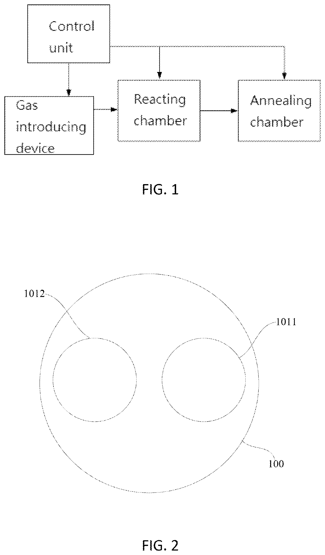
[0039]In light of aforesaid defects, a present invention according to the present invention provides a ALD apparatus, as shown in FIG. 1. The ALD apparatus comprises a reacting chamber, a gas introducing device connecting to the reacting chamber, an annealing chamber, and a control unit connecting to the reacting chamber, the gas introducing device and the annealing chamber. The gas introducing device connecting to the reacting chamber is used to provide rea...

second embodiment

[0051]A second embodiment provides an ALD apparatus. Referring to FIG. 1, the ALD apparatus comprises the reacting chamber, the gas introducing device connecting to the reacting chamber, the annealing chamber, and the control unit connecting to the reacting chamber, the gas introducing device and the annealing chamber. A bearing step is positioned at a bottom of the reacting chamber to bear the substrate to be deposited with the film. The gas introducing device connecting to the reacting chamber is used to provide reacting gases to the reacting chamber to carry out ALD. The control unit connecting to the gas introducing device is used to select the reacting gases provided by the gas introducing device and control parameters such as gas flow rate of the reacting gases, gas supply period, etc. The control unit connecting to the reacting chamber is used to control a temperature in the reacting chamber, temperature holding period, etc. The control unit connecting to the annealing chambe...

third embodiment

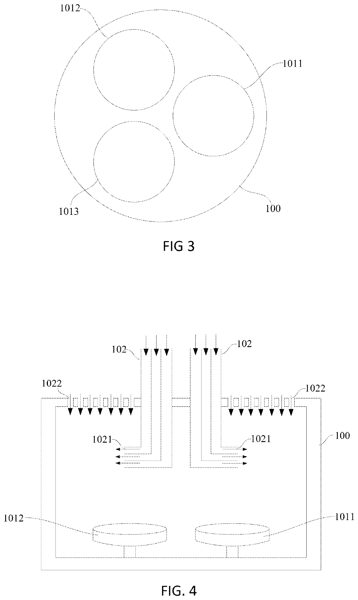
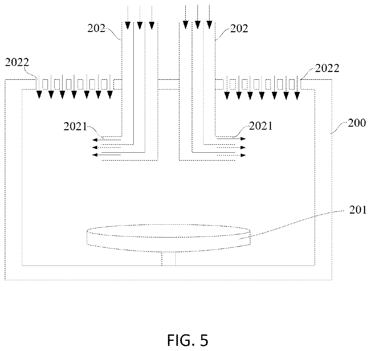
[0058]A third embodiment provides an ALD method which may apply one of the ALD apparatus disclosed in the first and second embodiments. Taking depositing a binary compound crystal for example, preferably, when depositing the binary compound crystal, the ALD apparatus shown in FIG. 4 is used. As shown in FIG. 6, the method may comprise steps of: step S101: placing the substrate to be deposited with a film on a first heater of a reacting chamber; step S102: moderating temperature of the first heater to heat the substrate; step S103: introducing a first reacting gas into the reacting chamber to form a first atomic layer on a surface of the substrate; and step S104: placing the substrate on a second heater of the reacting chamber; step S105: moderating temperature of the second heater to heat the substrate; step S106: introducing a second reacting gas into the reacting chamber to form a second atomic layer on the surface of the substrate, a surface reaction occurring at the second atomi...


PUM

PropertyMeasurementUnit
Temperatureaaaaaaaaaa
Thicknessaaaaaaaaaa

Abstract

The present invention relates to an ALD (Atomic layer deposition) apparatus and an ALD method. The ALD apparatus is provided with a reacting chamber and an annealing chamber, in which the reacting chamber is positioned with several heaters, a substrate to be deposited with an epitaxial layer may be transferred between different heaters, and each heater may independently moderate temperature. Different heaters correspond to different ALDs, and the number of the heaters may be varied to meet required a film to be deposited or composition of a crystal material. Because the heaters may be optimized to adapt to required temperature of different reactant gases, thickness of the epitaxial layer will meet expectation, and quality of the epitaxial layer will be promoted. Meanwhile, moderating the temperature independently may raise yield of production. Further, the ALD apparatus of the present invention introduces gas both horizontally and vertically to form a more even airflow field which benefits in forming a high-quality epitaxial layer.

Description

FIELD OF THE INVENTION[0001]The present invention relates to semiconductor devices and semiconductor apparatus, and specially relates to a new ALD (Atomic layer deposition) apparatus and a new ALD method.BACKGROUND OF THE INVENTION[0002]ALD (Atomic layer deposition) is a method of forming deposition film through alternately introducing gaseous precursor pulses into a reactor to generate chemical adhesion and reaction on a base. ALD may satisfy requirements of controlling atomic layers and holding a shape during deposition through the sequential and self-limiting surface reaction. ALD may benefits in controlling deposition thickness precisely, even to the extent of Angstrom (A) order or single layer of atoms, and excellent step coverage and conformal deposition through the self-limiting characteristic of ALD. The self-limiting characteristic and temperature of the surface reaction will cause unpredictable disappearance of the precursor flow rate, and so as to cause non-statistical de...

Claims


Application Information

Patent Timeline
IPC IPC(8): C30B25/14H01L21/02C23C16/455C23C16/32C30B25/10C30B25/12C30B33/02C30B29/36
CPCC30B25/14H01L21/0262H01L21/02529C23C16/45544C30B29/36C30B25/10C30B25/12C30B33/02C23C16/325C23C16/45525C23C16/45548C23C16/52C23C16/46C23C16/45502C23C16/45565
Inventor MENG, ZHAOSHENGWU, ZHUANGZHUANGCHI, MIN-HWA
Owner SIEN QINGDAO INTEGRATED CIRCUITS CO LTD
Why Eureka
Try Eureka