Gallium nitride substrate and optical device using the same

a technology of gallium nitride and substrate, which is applied in the direction of semiconductor/solid-state device testing/measurement, instruments, semiconductor lasers, etc., can solve the problems of deterioration of poor crystal quality of epitaxial growth layer, and decrease in yield, so as to reduce residual carbon and enhance the crystalline quality of epitaxial layer grown on gallium nitride substrate.

Inactive Publication Date: 2013-09-05
SUMITOMO CHEM CO LTD
View PDF2 Cites 2 Cited by
  • Summary
  • Abstract
  • Description
  • Claims
  • Application Information

AI Technical Summary

Benefits of technology

[0018]According to one embodiment of the invention, a gallium nitride(GaN) substrate is constructed so as to satisfy the GaLα / CKα peak intensity ratio of not less than 2. Based on the GaLα / CKα peak intensity ratio which is calculated as an amount of C (carbon) with respect to Ga, an increase or decrease in the amount of residual carbon can be determined so as to evaluate the amount of residual carbon on the surface of the GaN substrate. By satisfying the above GaLα / CKα peak intensity ratio, it is possible to obtain the gallium nitride substrate with the reduced amount of residual carbon on the surface thereof. Thus, the crystalline quality of an epitaxial layer grown on the gallium nitride substrate can be enhanced.

Problems solved by technology

However, crystal quality of an epitaxial growth layer is poor is case of epitaxial growth using the GaN substrate polished by the method of JP-A-2001-322899 and an optical device using such a substrate has a problem that emission intensity decreases, which causes failure and a decrease in a yield.
As a result of intensive examination of this problem, it was found that the diamond used as the loose abrasive is embedded into and remains on the surface of the GaN substrate when the GaN substrate is polished and crystal quality of the epitaxial growth layer deteriorates due to a carbon component of the diamond.
It is also found that the wax used when polishing remains and the crystal quality deteriorates due to a carbon component of the wax.

Method used


Image

  • Gallium nitride substrate and optical device using the same
  • Gallium nitride substrate and optical device using the same
  • Gallium nitride substrate and optical device using the same

Examples


example 1

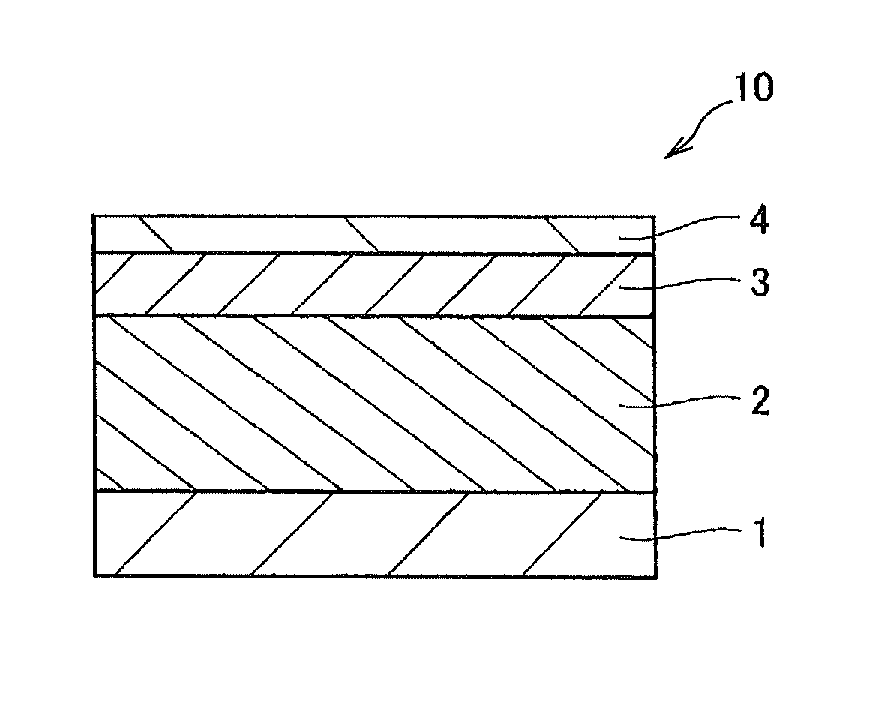
[0050]In Example 1, a GaN single crystal was grown by the VAS method to make a GaN substrate.

[0051]Firstly, a void-containing substrate was prepared. For making the void-containing substrate, a 500 nm-thick GaN base layer was formed on a sapphire substrate (3.5 inches in diameter) by the MOVPE method, etc., a 30 nm-thick Ti layer was deposited on a surface thereof, and subsequently, heat treatment (at a temperature of 1000° C.) was carried out in a mixture gas of H2 and NH3 for 30 minutes to form voids in the GaN layer while converting the Ti layer into TiN having a mesh structure.

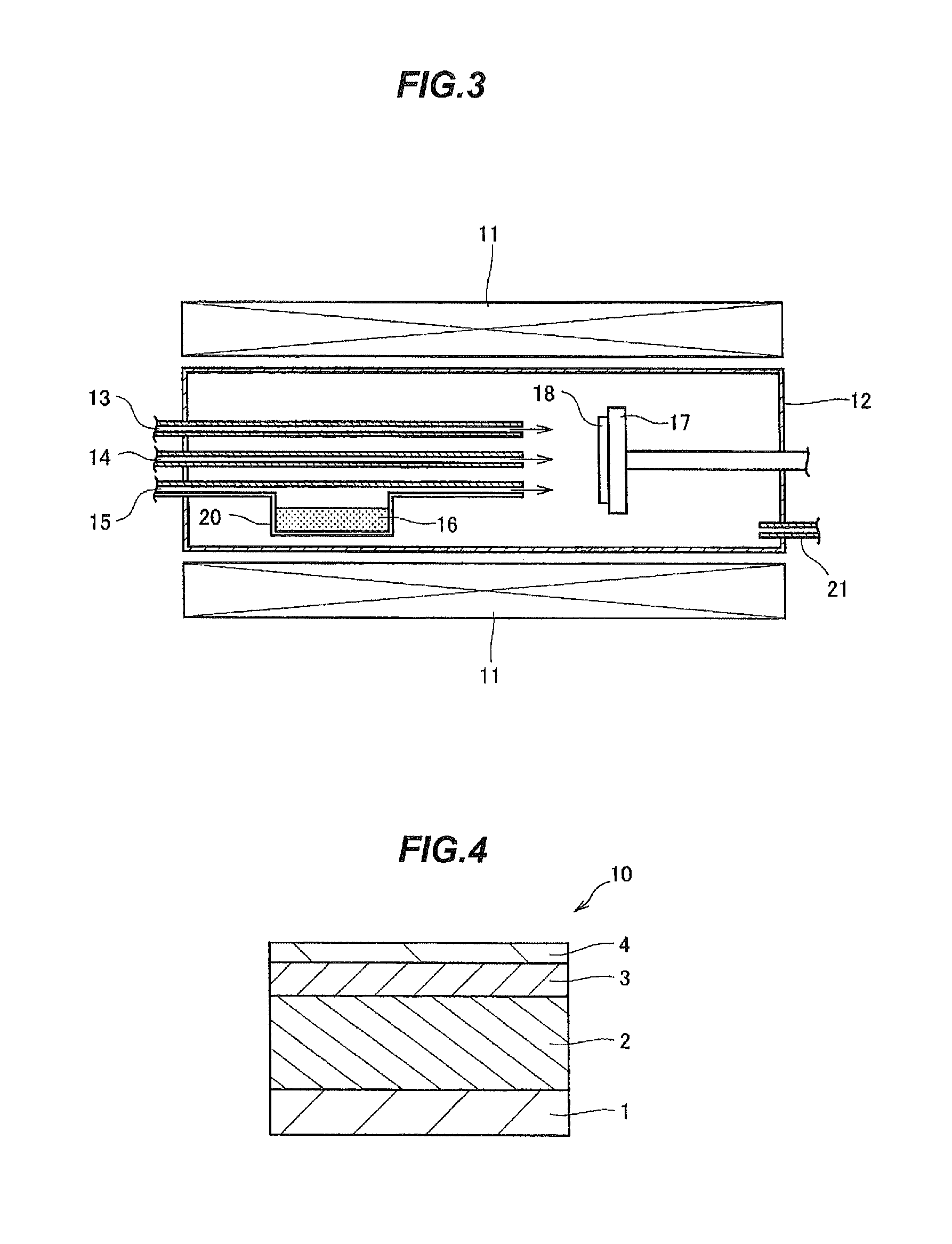
[0052]The void-containing substrate was placed on the substrate holder 17 in the HVPE apparatus shown in FIG. 3, and was heated in the reaction tube 12 at atmospheric pressure so as to have a substrate temperature of 1050° C. The initial nucleation conditions were as follows: 5×10⁻² atm of NH3 gas was introduced together with 6×10⁻¹ atm of N2 gas as a carrier gas from the reaction gas inlet tube 13, 5×10⁻³...


PUM

PropertyMeasurementUnit
accelerating voltageaaaaaaaaaa
temperatureaaaaaaaaaa

Abstract

A gallium nitride substrate that a GaLα / CKα peak intensity ratio in EDX spectrum is not less than 2. The EDX spectrum is obtained in energy dispersive X-ray microanalysis (EDX) of a surface of the gallium nitride substrate using a scanning electron microscope (SEM) at an accelerating voltage of 3 kV.

Description

[0001]The present application is based on Japanese patent application No. 2012-047203 filed on Mar. 2, 2012, the entire contents of which are incorporated herein by reference.BACKGROUND OF THE INVENTION[0002]1. Field of the Invention[0003]The invention relates to a gallium nitride substrate and an optical device using the gallium nitride substrate.[0004]2. Description of the Related Art[0005]GaN-based semiconductor crystals such as gallium nitride (GaN) has attracted attention as a material of optical devices such as light emitting diode (LED) which emits high-intensity blue light or long-life laser diode (LD) which emits blue light.[0006]Bulk crystal growth of the GaN-based semiconductor crystals is difficult, and accordingly, it is difficult to produce a large single crystal GaN with high quality. However, in recent years, a method of manufacturing a GaN-based semiconductor crystal has been proposed, using a DEEP (Dislocation Elimination by the Epi-growth with Inverted-Pyramidal P...

Claims


Application Information

Patent Timeline
Patent Type & Authority Applications(United States)
IPC IPC(8): C01B21/06
CPCC30B25/00H01L33/32C01B21/0632C30B29/406H01S5/0206H01S5/32341H01L33/0075G01N23/2252H01L21/02057H01L21/30612H01L21/30625H01L22/12H01L29/2003
Inventor YAMAMOTO, SHUNSUKE
Owner SUMITOMO CHEM CO LTD
Why Eureka
Try Eureka