Method of fabricating semiconductor device using gang bonding and semiconductor device fabricated by the same

a technology of gang bonding and semiconductor devices, which is applied in the direction of semiconductor devices, semiconductor/solid-state device details, electrical devices, etc., can solve the problems of difficult uniform formation of resin, complicated process of fabricating led packages, and long time for fabricating led packages, so as to achieve rapid fabrication of led packages and avoid failure of led packages

Active Publication Date: 2015-09-24
LEE CHUNG HOON +2
View PDF2 Cites 4 Cited by
  • Summary
  • Abstract
  • Description
  • Claims
  • Application Information

AI Technical Summary

Benefits of technology

This patent text is about a new method for making LED packages. The current method involves individually bonding LED chips to a circuit board and adding wires, which makes the process complicated and time-consuming. This new method simplifies the process and allows for faster and more efficient fabrication of LED packages. Additionally, the new method ensures stable electrical connections between the LED chips' electrode pads and the external lead terminals. The text describes the challenges with conventional methods and highlights the technical effects of the new method.

Problems solved by technology

Meanwhile, in a case where an LED chip is covered with a resin containing phosphor at a package level, the phosphor is not uniformly dispersed into the resin, and further, it is difficult to uniformly form the resin.
Hence, a process of fabricating LED packages is complicated, and it takes much time to fabricate the LED packages.
Further, a wire bonding process using a capillary requires a space for moving the capillary, and hence the space acts as a limitation in miniaturizing the LED packages.
Furthermore, failure of the LED packages is easily caused by bonding failure of wires, disconnection, or the like.

Method used


Image

  • Method of fabricating semiconductor device using gang bonding and semiconductor device fabricated by the same
  • Method of fabricating semiconductor device using gang bonding and semiconductor device fabricated by the same
  • Method of fabricating semiconductor device using gang bonding and semiconductor device fabricated by the same

Examples


first embodiment

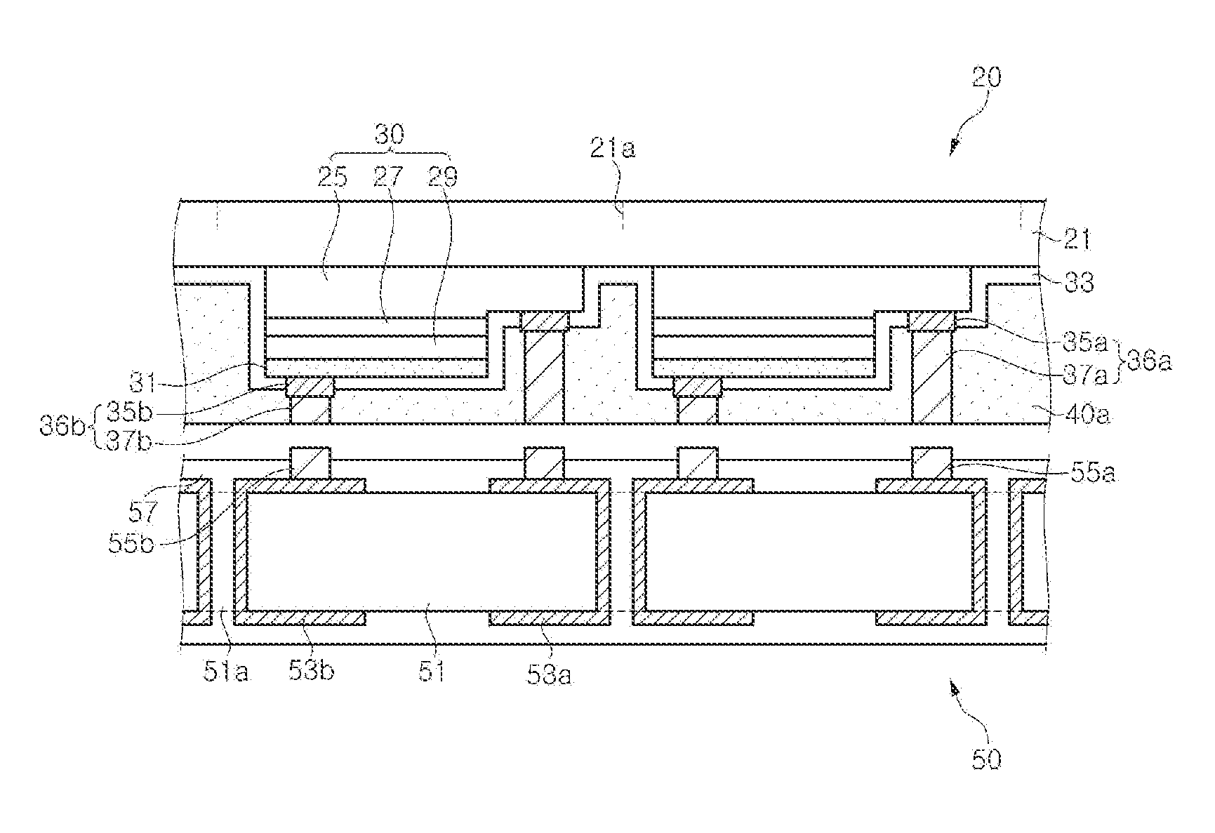
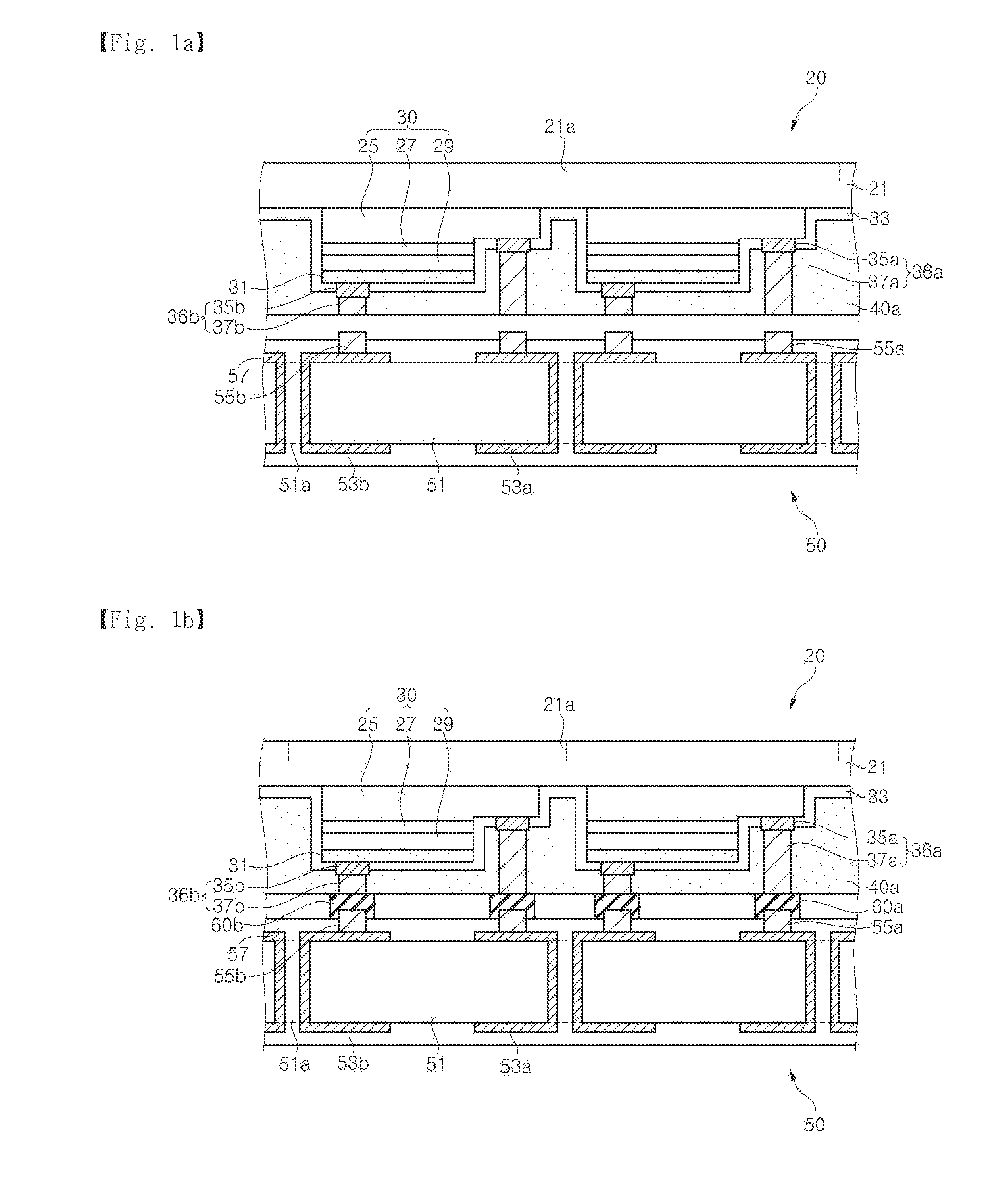
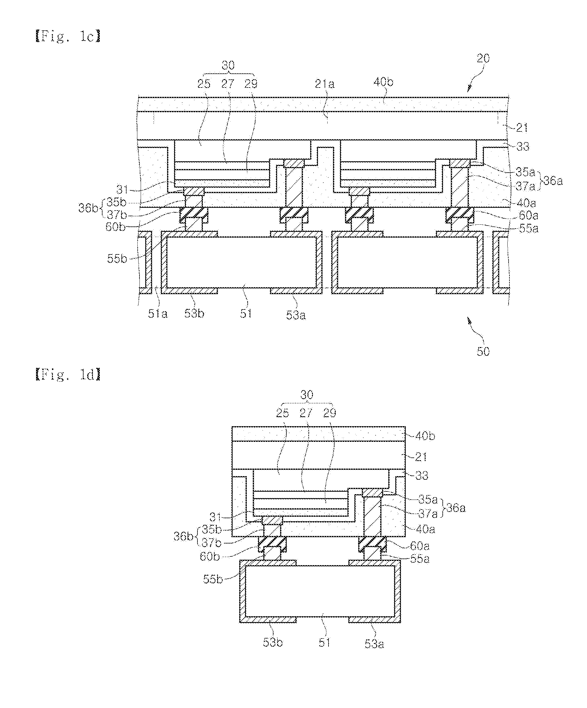
[0057]FIGS. 1a to 1d are sectional views illustrating a method of fabricating an LED package according to the present invention.

[0058]Referring to FIG. 1d, there is provided a substrate assembly 20 in which a plurality of semiconductor stack structures 30 are arrayed on a substrate 21, and there is a packaging member 50 having lead electrodes 53a and 53b.

[0059](Preparation of Substrate Assembly 20)

[0060]The substrate assembly 20 may comprise a substrate 21, semiconductor stack structures 30, a first electrode 36a, a second electrode 36b and a first wavelength converter 40a. Each of the semiconductor stack structures may comprise a first conductive semiconductor layer 25, an active layer 27 and a second conductive semiconductor layer 29. The first electrode 36a may comprise a first electrode pad 35a and a first additional electrode 37a, and the second electrode 36b may comprise a second electrode pad 35b and a second additional electrode 37b.

[0061]The substrate assembly 20 may comp...

second embodiment

[0095]FIGS. 3a to 3d are sectional views illustrating a method of fabricating an LED package according to the present invention.

[0096]Referring to FIG. 3a, a substrate assembly 20a according to this embodiment is different from the substrate assembly 20 of Fig. la in that the first wavelength converter 40a is not formed. An anti-plating layer 67 may be formed in place of the first wavelength converter 40a. Like the anti-plating layer 57, the anti-plating layer 67 may be formed of photoresist, polyimide or the like.

[0097]Referring to FIG. 3b, as described with reference to FIG. 1b, a first plating layer 60a is formed between the first electrode 36a and the first spacer electrode 55a, and a second plating layer 60a is formed between the second electrode 36b and the second spacer electrode 55b.

[0098]Referring to FIG. 3c, after the plating layers 60a and 60b are formed, the anti-plating layers 57 and 67 are removed using acetone or the like. Then, a first wavelength converter 70a is fo...

third embodiment

[0101]FIGS. 4a and 4b are sectional views illustrating a method of fabricating an LED package according to the present invention.

[0102]Referring to FIG. 4a, a substrate assembly 20b according to this embodiment is almost identical to the substrate assembly 20 described with reference to FIG. 1a, but is different in that the first conductive semiconductor layer 25 is not separated for each of the semiconductor stack structures 30 but continuous. That is, when the epitaxial layers formed on the growth substrate 21 are patterned, some regions of the second conductive semiconductor layer 29 and the active layer 27 are removed, and the first conductive semiconductor layer 25 is partially patterned.

[0103]Subsequent processes are performed identically to those described with reference to FIGS. 1a to 1d. Accordingly, when the growth substrate 21 is divided, the first conductive semiconductor layer 25 is divided together with the growth substrate, and thus side surfaces of the growth substra...


PUM


Abstract

A semiconductor device including a first lead electrode and a second lead electrode; a semiconductor stack structure disposed on the member, the semiconductor stack structure including a first conductive semiconductor layer, a second conductive semiconductor layer, and an active region interposed between the first and second conductive semiconductor layers; a first electrode electrically connected to the first conductive semiconductor layer; a second electrode electrically connected to the second conductive semiconductor layer; a plating layer configured to bond the semiconductor stack structure to the member; and a first wavelength converter that covers at least side surfaces of the semiconductor stack structure.

Description

CROSS-REFERENCE TO RELATED APPLICATIONS[0001]This is a Continuation of U.S. patent application Ser. No. 13 / 992,941, filed on Jun. 10, 2013, which is the National Stage entry of International Application PCT / KR2011 / 004776, filed on Jun. 30, 2011, and claims priority from and the benefit of Korean Patent Application No. 10-2010-0126218, filed on Dec. 10, 2010, which are incorporated herein by reference for all purposes as if fully set forth herein.BACKGROUND[0002]1. Field[0003]The present invention relates to a method of fabricating a semiconductor device and a semiconductor device, and more particularly, to a method of fabricating a semiconductor device using gang bonding and a semiconductor device fabricated by the same.[0004]2. Discussion of the Background[0005]Light emitting diodes (LEDs) can be made light in weight, thin in thickness and small in size, and have advantages of energy saving and long lifespan. Accordingly, the LEDs are used as backlight sources for various types of ...

Claims


Application Information

Patent Timeline
Patent Type & Authority Applications(United States)
IPC IPC(8): H01L33/50H01L33/44H01L33/36
CPCH01L33/507H01L33/44H01L33/36H01L33/0095H01L2924/01029H01L2224/27462H01L2224/81893H01L2224/83893H01L24/05H01L24/06H01L24/27H01L24/32H01L24/33H01L24/83H01L24/94H01L2224/04026H01L2224/05073H01L2224/05124H01L2224/05144H01L2224/05147H01L2224/05155H01L2224/05171H01L2224/05553H01L2224/05571H01L2224/06151H01L2224/32238H01L2224/325H01L2224/83447H01L2224/83455H01L2224/94H01L2224/97H01L2224/33151H01L33/486H01L2933/0033H01L2924/12041H01L2924/15787H01L2924/12042H01L33/0093H01L2924/00012H01L2924/00014H01L2224/81H01L2924/01028H01L2924/01047H01L2924/00H01L23/49805H01L2224/11462H01L2224/16057H01L2224/16151H01L2224/16013H01L24/11H01L24/16H01L33/005H01L33/50
Inventor LEE, CHUNG HOONKAL, DAE SUNGNAM, KI BUM
Owner LEE CHUNG HOON
Why Eureka
Try Eureka