Wafer level light-emitting diode array

a technology of light-emitting diodes and arrays, which is applied in the direction of basic electric elements, electrical equipment, and semiconductor devices, can solve the problems of increasing the fabrication cost of an illuminating apparatus including the light-emitting diodes, the inability to use the light-emitting diodes directly under the common ac power source, and the loss of light, so as to improve the current distribution performance, improve reliability, and reduce the loss of light

Active Publication Date: 2015-10-01
SEOUL VIOSYS CO LTD
View PDF11 Cites 24 Cited by
  • Summary
  • Abstract
  • Description
  • Claims
  • Application Information

AI Technical Summary

Benefits of technology

[0036]According to embodiments of the present invention, it is possible to provide a light emitting diode array on a wafer level, which can be driven at a high voltage and can be mounted directly on a printed circuit board or the like. In particular, since light emitting diodes of the light emitting diode array are connected in series by upper electrodes, a submount substrate is not required. Since the upper electrode can include an ohmic contact layer, it is not necessary to form a separate ohmic contact layer.
[0037]In addition, side surfaces of the light emitting diodes are formed to be inclined at a predetermined angle, so that it is possible to provide a flip-chip type light emitting diode array on a wafer level, which has improved reliability. Further, the side surfaces of the lower electrodes, first interlayer insulating layer, upper electrodes or second interlayer insulating layer are formed to be inclined at a predetermined angle, so that it is possible to prevent cracks from being produced in another layer formed on the respective layers.
[0038]Further, since the upper electrodes occupy a relatively large area, and also cover side surfaces of the light emitting diodes and most of the regions between the light emitting diodes, the upper electrodes can be used to reflect light. Thus, it is possible to reduce a loss of light generated in the regions between the light emitting diodes. Therefore, it is not necessary to additionally form a separate reflective metal layer for reflecting light, in addition to the upper electrodes.
[0039]Furthermore, the upper electrodes are made in the form of a plate or sheet having a wide area, thereby improve current distribution performance and decreasing a forward voltage at an identical current while using an identical number of light emitting diodes.

Problems solved by technology

Therefore, the light emitting diode has a disadvantage in that it cannot be used directly under the common AC power source of 110V or 220V.
Accordingly, a driving circuit for the light emitting diode should be provided, which becomes one factor causing fabrication costs of an illuminating apparatus including the light emitting diode to be increased.
Since a discrete driving circuit should be provided, the volume of the illuminating apparatus is increased and unnecessary heat is generated.
In addition, there are problems such as improvement of a power factor for the supplied power.
Therefore, there are problems in that a processing time for constructing the array is increased, and fabrication costs of the array are increased.
Accordingly, there is a problem in that a molding process of forming the molding layer is additionally required, resulting in increase in the complexity of processes.
Particularly, in a case of application of a chip type with a lateral structure, the light-emitting performance of the light emitting diode chip is lowered, and the quality of the light emitting diode is deteriorated due to the generation of heat.
However, the air bridge connection structure results in weak durability and the lateral type causes a problem of deterioration of the light-emitting performance or heat-dissipating performance.
On the contrary, the use of the submount substrate causes increase in both fabrication costs and the thickness of a final product.
In addition, there are further disadvantages of needs for an additional wiring process for the submount substrate and an additional process of mounting the submount substrate on a new substrate.
To this end, various kinds of masks should be used, which becomes a problem.
In addition, exfoliation or crack occurs due to a difference in thermal expansion coefficient between the n-electrode and the interconnection electrode, or the like, and therefore, there is a problem in that electrical contact therebetween is opened.

Method used


Image

  • Wafer level light-emitting diode array
  • Wafer level light-emitting diode array
  • Wafer level light-emitting diode array

Examples


Embodiment Construction

[0058]Hereinafter, preferred embodiments of the present invention will be described in greater detail with reference to the accompanying drawings, in order to more fully describe the present invention. However, the present invention is not limited to the following embodiments but may be implemented in other forms.

[0059]In these embodiments, it will be understood that the term “first”, “second”, “third” or the like does not impose any limitation on components but are only used to distinguish the components.

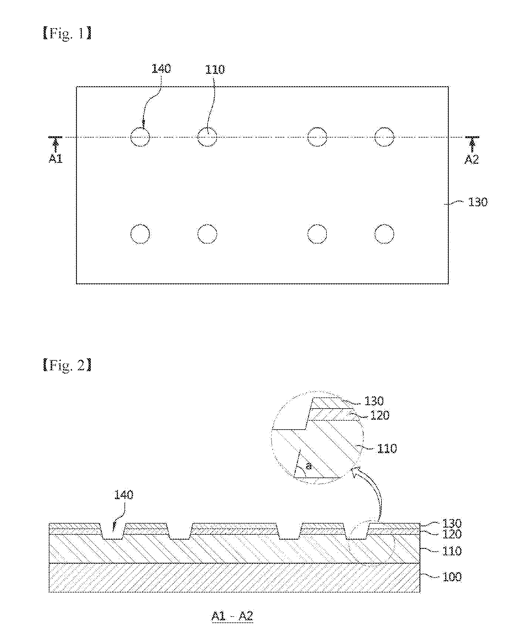
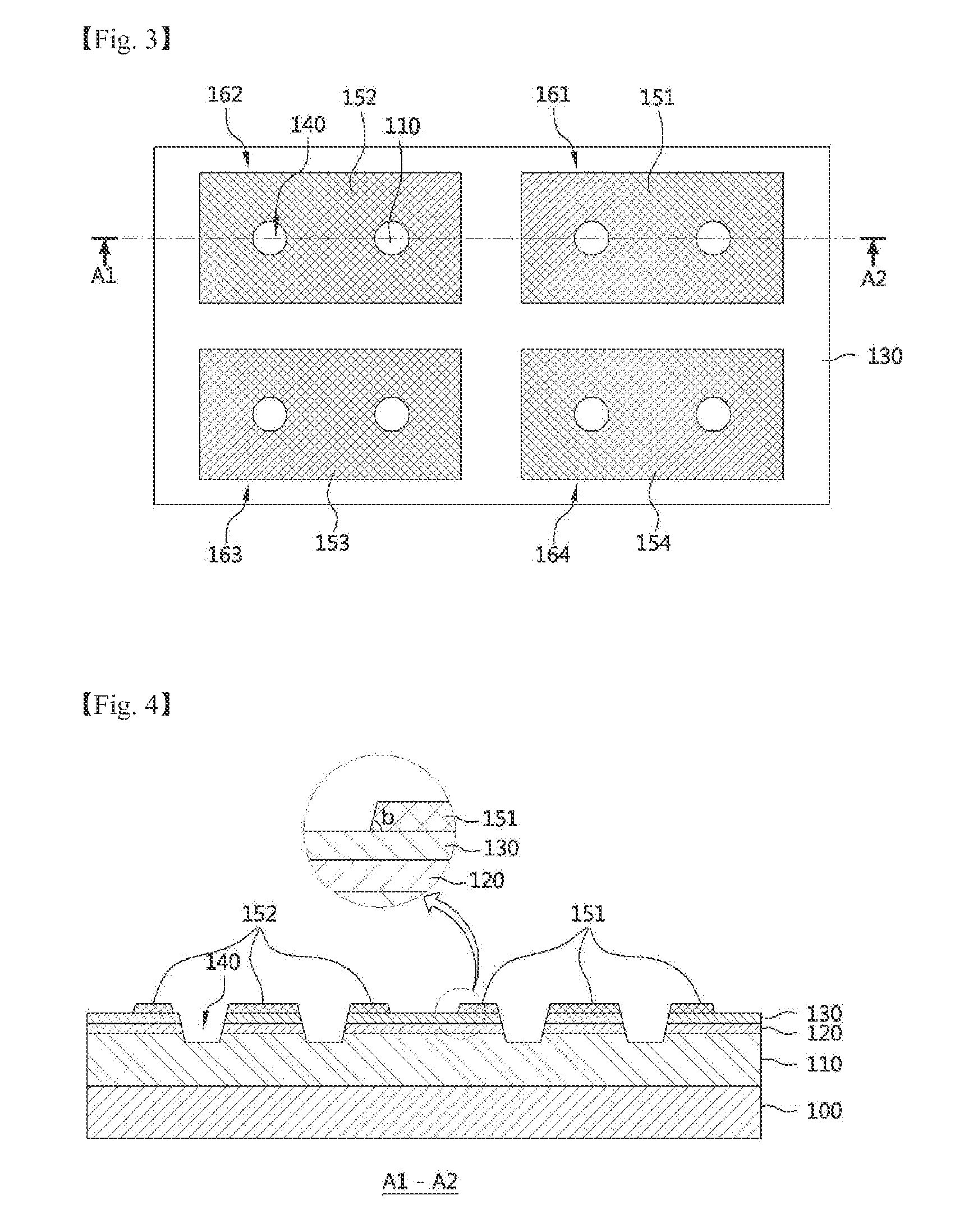
[0060]FIGS. 1 and 2 are plan and sectional views showing that a plurality of via holes are formed in a laminated structure according to an embodiment of the present invention.

[0061]In particular, FIG. 2 is a sectional view taken along line A1-A2 in the plan view of FIG. 1.

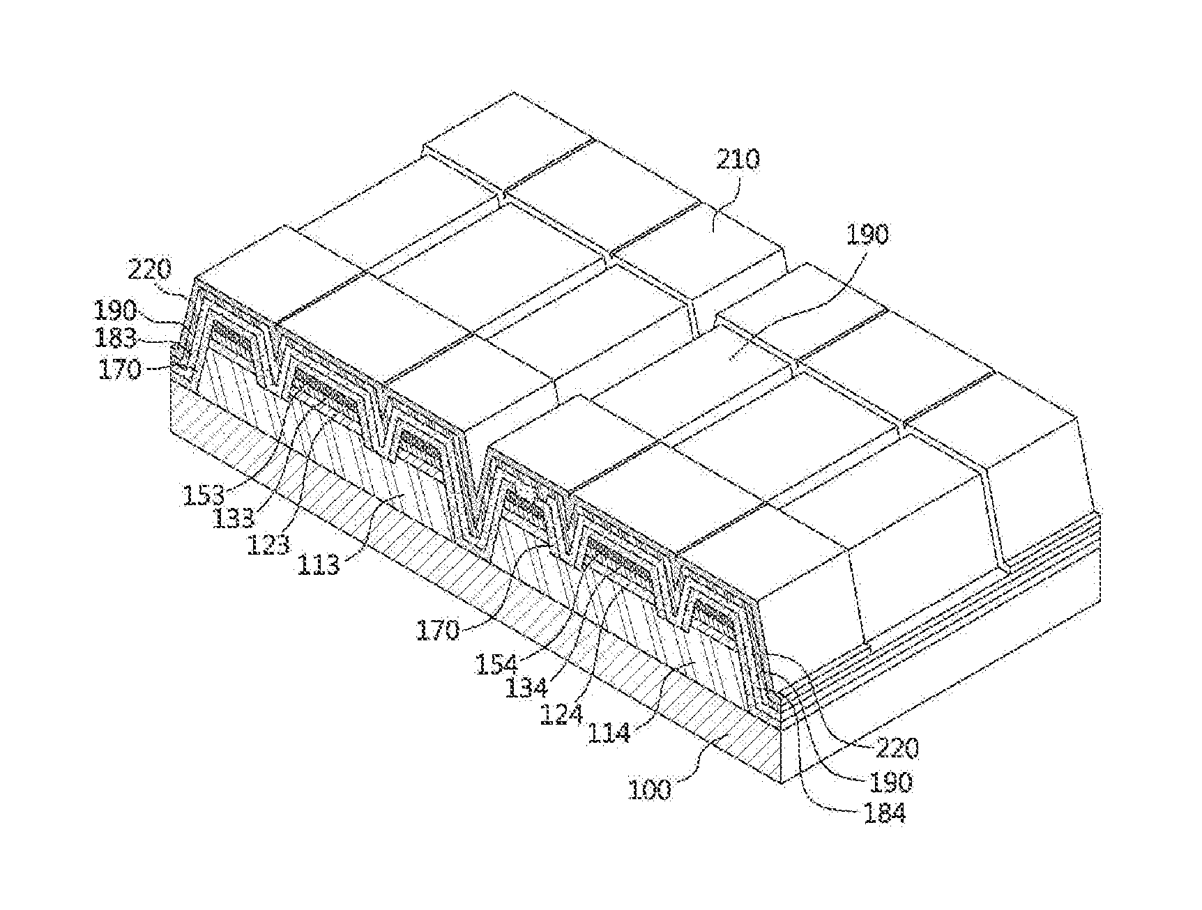
[0062]Referring to FIGS. 1 and 2, a first semiconductor layer 110, an active layer 120 and a second semiconductor layer 130 are formed on a substrate 100, and via holes 140 are formed to allow a surface of the sem...


PUM


Abstract

A wafer level light-emitting diode (LED) array includes: a growth substrate; a plurality of LEDs arranged over the substrate, each including a first semiconductor layer, an activation layer, and a second semiconductor layer; a plurality of upper electrodes formed from a common material and electrically connected to the first semiconductor layers of the corresponding LEDs; and first and second pads arranged over the upper electrodes. The LEDs are connected in series by the upper electrodes, the first pad is electrically connected to an input LED from among the LEDs connected in series, and the second pad is electrically connected to an output LED from among the LEDs connected in series. Accordingly, a flip chip-type LED array can be provided which can be driven with a high voltage.

Description

TECHNICAL FIELD[0001]The present invention relates to a light emitting diode array, and more particularly, to a light emitting diode array with a plurality of light emitting diodes connected through wires and formed into a flip chip type.BACKGROUND ART[0002]A light emitting diode is a device for performing a light emitting operation when a voltage of a turn-on voltage or more is applied thereto through anode and cathode terminals thereof. Generally, the turn-on voltage for causing the light emitting diode to emit light has a value much lower than the voltage of a common power source. Therefore, the light emitting diode has a disadvantage in that it cannot be used directly under the common AC power source of 110V or 220V. The operation of the light emitting diode using the common AC power source requires a voltage converter for lowering the supplied AC voltage. Accordingly, a driving circuit for the light emitting diode should be provided, which becomes one factor causing fabrication...

Claims


Application Information

Patent Timeline
Patent Type & Authority Applications(United States)
IPC IPC(8): H01L33/62H01L33/38H01L33/40H01L27/15
CPCH01L33/62H01L33/405H01L33/38H01L27/153H01L27/156H01L2933/0016H01L33/44H01L33/40H01L33/382H01L2924/0002H01L2924/00
Inventor JANG, JONG MINCHAE, JONG HYEONLEE, JOON SUPSUH, DAEWOONGKIM, HYUN A.ROH, WON YOUNGKANG, MIN WOO
Owner SEOUL VIOSYS CO LTD
Why Eureka
Try Eureka