
Precision Measurement of Voltage Drop Across a Semiconductor Switching Element

a technology of switching element and voltage drop, which is applied in the direction of power supply testing, pulse technique, instruments, etc., can solve the problems of circuit b>100/b> not providing sufficient precision for determining the aging of the igbt, damage the measurement circuit, etc., and achieves the effect of convenient and inexpensiv

Active Publication Date: 2015-10-22
SIEMENS ENERGY AS
View PDF46 Cites 3 Cited by
  • Summary
  • Abstract
  • Description
  • Claims
  • Application Information

AI Technical Summary

Benefits of technology

The patent text describes an apparatus for measuring the voltage between two terminals of a semiconductor switching element. This apparatus uses a protective element to prevent current flow when the switching element is not conducting, which allows for accurate voltage measurement when the switching element is conducting. This technology, which is similar to existing methods, allows for high-precision measurement of voltage across the switching element, which can help analyze its aging state and estimate its remaining lifetime. The technical effect of this patent is to provide a simple and cost-effective way of accurately measuring voltage and analyzing the performance of semiconductor switches, which can be useful for the design and maintenance of subsea devices.

Problems solved by technology

The measurement circuit is by nature a high-impedance circuit, and therefore the current source will set up a high voltage, which may damage the measurement circuit.
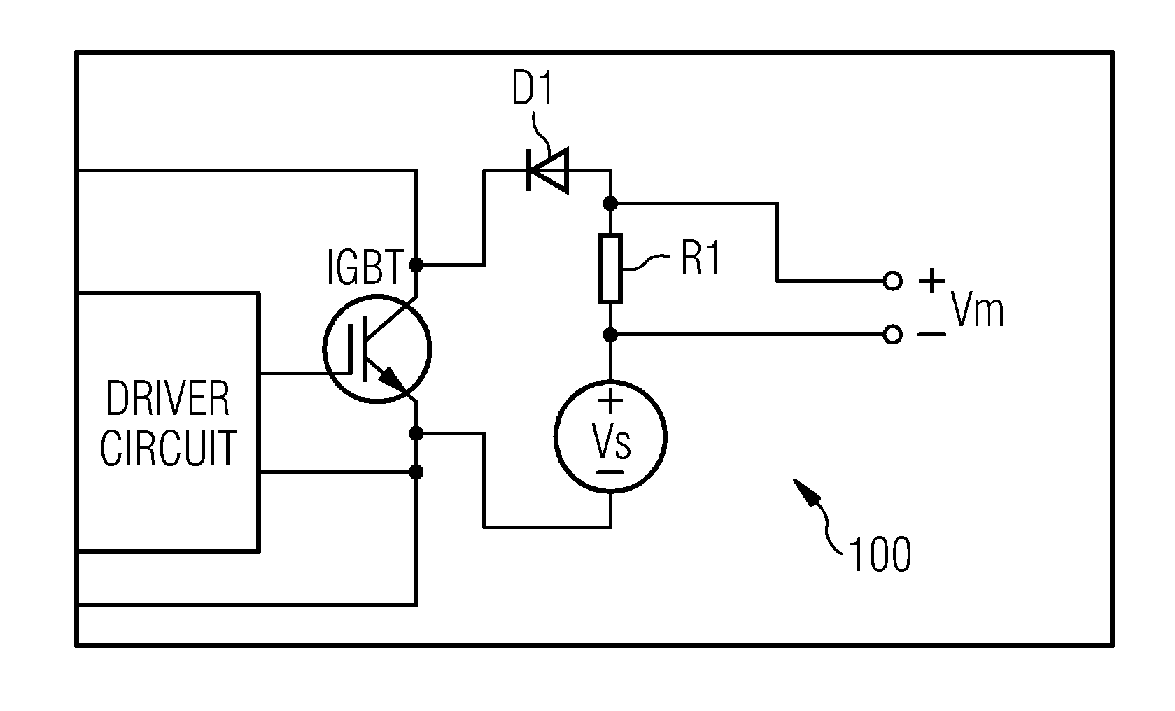
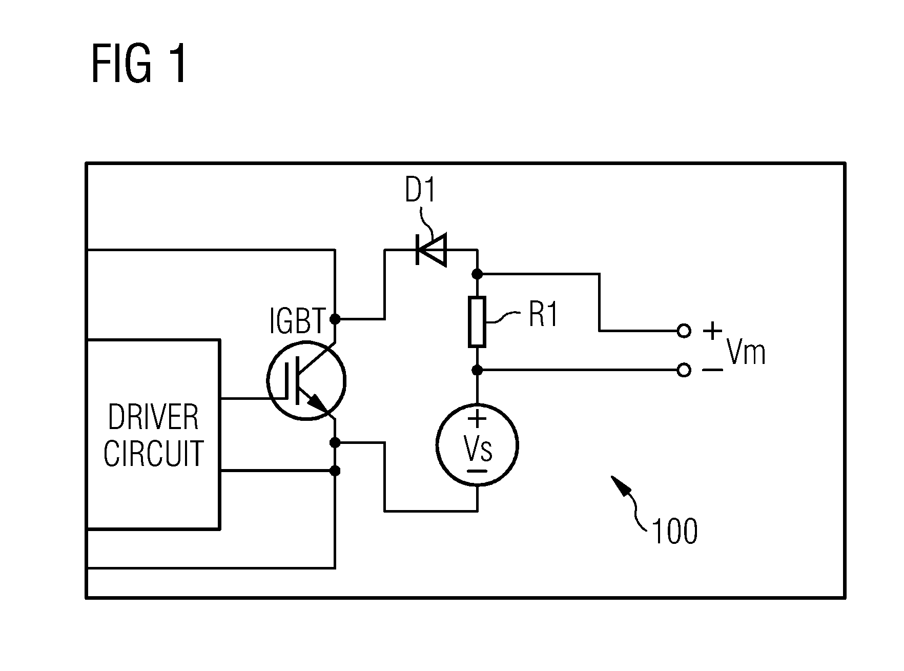
Therefore, a Vce measurement based on the circuit 100 may not provide sufficient precision for determining the aging of the IGBT.

Method used


Image

  • Precision Measurement of Voltage Drop Across a Semiconductor Switching Element
  • Precision Measurement of Voltage Drop Across a Semiconductor Switching Element
  • Precision Measurement of Voltage Drop Across a Semiconductor Switching Element

Examples


Embodiment Construction

[0048]The illustration in the drawing is schematic. It is noted that in different figures, similar or identical elements are provided with the same reference numerals or with reference numerals which differ only within the first digit.

[0049]FIG. 1 shows a circuit 100 for estimating a collector-emitter voltage drop of an IGBT according to the prior art. The circuit 100 has already been discussed in the introduction and will therefore not be discussed further here.

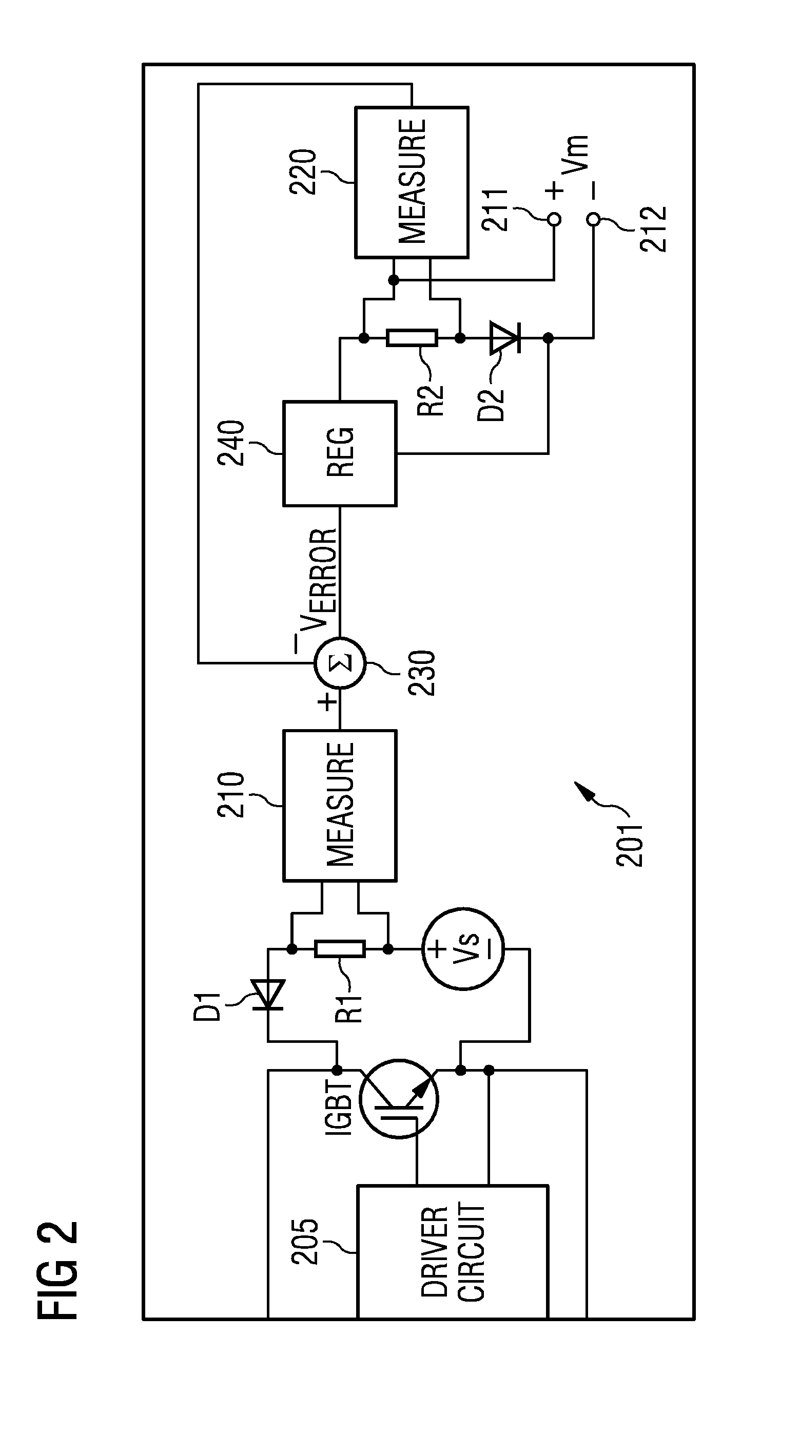
[0050]FIG. 2 shows a principal circuit diagram of an apparatus 201 for precision measurement of a collector-emitter voltage drop of an IGBT in accordance with an embodiment. As shown, the gate terminal of the IGBT is connected to driver circuit 205 of a subsea adjustable speed drive device. The IGBT is coupled to act as a switch and is driven with a switching frequency between 200 Hz and 1200 Hz, where the nominal frequency is 600 Hz. When the IGBT is not conducting, the collector-emitter voltage is about 1 kV. It is noted t...


PUM


Abstract

An apparatus provides precision measurement of voltage drop across a semiconductor switching element of a subsea device. The apparatus includes (a) a first circuit path having a first protective element, a first impedance element and a voltage source, wherein the first circuit path is configured to be connected between the first terminal and the second terminal of the semiconductor switching element, (b) a second circuit path formed between a first output terminal and a second output terminal, the second circuit path having a second protective element and a second impedance element, wherein the second protective element is identical to the first protective element, and wherein the second impedance element is identical to the first impedance element, and (c) a regulating circuit configured to regulating the current in the second circuit path such that said current in the second circuit path is equal to the current in the first circuit path, wherein the voltage drop between the first terminal and the second terminal of the semiconductor switching element equals the difference between the voltage provided by the voltage source and the voltage drop between the first output terminal and the second output terminal.

Description

RELATED CASE[0001]This application claims the benefit of EP 14165224.8, filed on Apr. 17, 2014, which is hereby incorporated by reference in its entirety.FIELD[0002]The present embodiments relate to the field of measurement of voltage drop across a semiconductor switching element, in particular to an apparatus for precision measurement of such voltage drop. The present embodiments further relate to a subsea device including the aforementioned apparatus, a system for monitoring a subsea device, and a method of precision measurement of voltage drop across a semiconductor switching element.BACKGROUND[0003]Many electrically powered systems, such as adjustable speed drives (ASDs) for subsea applications in connection with, for example, oil and gas production, utilize semiconductor switching elements, such as insulated-gate bipolar transistors (IGBTs). For instance, IGBTs may be used in DC-AC converters. In subsea applications where IGBTs and other components are not accessible once a dev...

Claims


Application Information

Patent Timeline
IPC IPC(8): G01R31/26H02M1/00
CPCG01R31/2642G01R31/2608G01R31/42G01R19/0084G01R31/2617H03K2217/0027
Inventor DAS, ANANDARUPLYSFJORD, IVAR HAAKON
Owner SIEMENS ENERGY AS
Learn More