Method for manufacturing semiconductor device

a semiconductor chip and manufacturing method technology, applied in semiconductor devices, semiconductor/solid-state device details, electrical equipment, etc., can solve the problems of deterioration of moisture resistance reliability, deterioration of electrical connection reliability, solder ball cannot cope with semiconductor chip multi-pin constitution, etc., to achieve excellent connection reliability, easy and inexpensive

Inactive Publication Date: 2009-10-22
LAPIS SEMICON CO LTD
View PDF3 Cites 24 Cited by
  • Summary
  • Abstract
  • Description
  • Claims
  • Application Information

AI Technical Summary

Benefits of technology

[0016]The present invention relates to improvement of the method for manufacturing the semiconductor device, and an object of the invention is to provide a method for manufacturing semiconductor device which enables manufacturing of a double-sided electrode package having a structure with excellent connection reliability and moisture-resistant reliability with respect to another package more easily and inexpensively than a case using the conventional resin sealing method such as the transfer molding method.
[0030]According to the invention, the double-sided electrode package where reliability of connection to another package and moisture-resistant reliability are excellent may be manufactured more simply and inexpensively than a case of using a conventional resin sealing method such as a transfer molding method.

Problems solved by technology

However, the conventional POP has the following various problems, for example:(1) since the packages are laminated, a mounting height should not be lower than a stack of semiconductor chips;(2) when the packages are warped, electric connection reliability is deteriorated;(3) since sealing of the lower package is not sufficient, moisture-resistant reliability is deteriorated; and(4) since reduction in a diameter of the solder balls provided as the connection terminals onto the package is limited, the solder balls cannot cope with a multi-pin constitution of the semiconductor chips.
These problems arise from the structure of the packages to be laminated.

Method used


Image

  • Method for manufacturing semiconductor device
  • Method for manufacturing semiconductor device
  • Method for manufacturing semiconductor device

Examples


first exemplary embodiment

[0052]A first exemplary embodiment describes a method for manufacturing double-sided electrode package where a semiconductor chip is mounted to a package substrate formed with plural surface-side terminals having plural protruded rims on an entire periphery of their side surfaces along a peripheral direction, and the semiconductor chip is sealed by liquid resin. The first exemplary embodiment describes manufacturing steps of forming the structure of the double-sided electrode package on a substrate frame formed with plural package substrates so as to divide (separate) the substrate frame into individual double-sided electrode packages.

[Double-Sided Electrode Package]

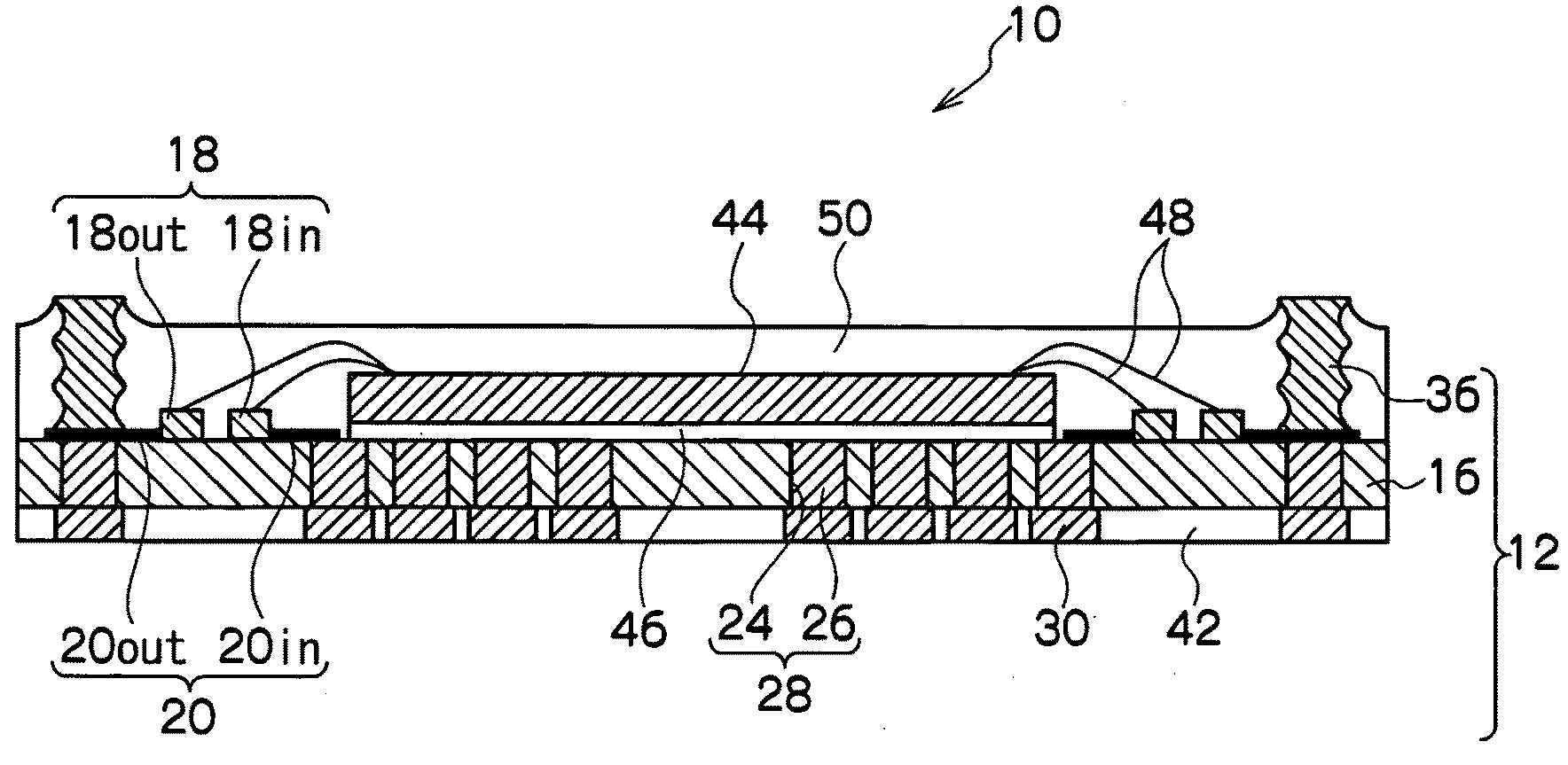
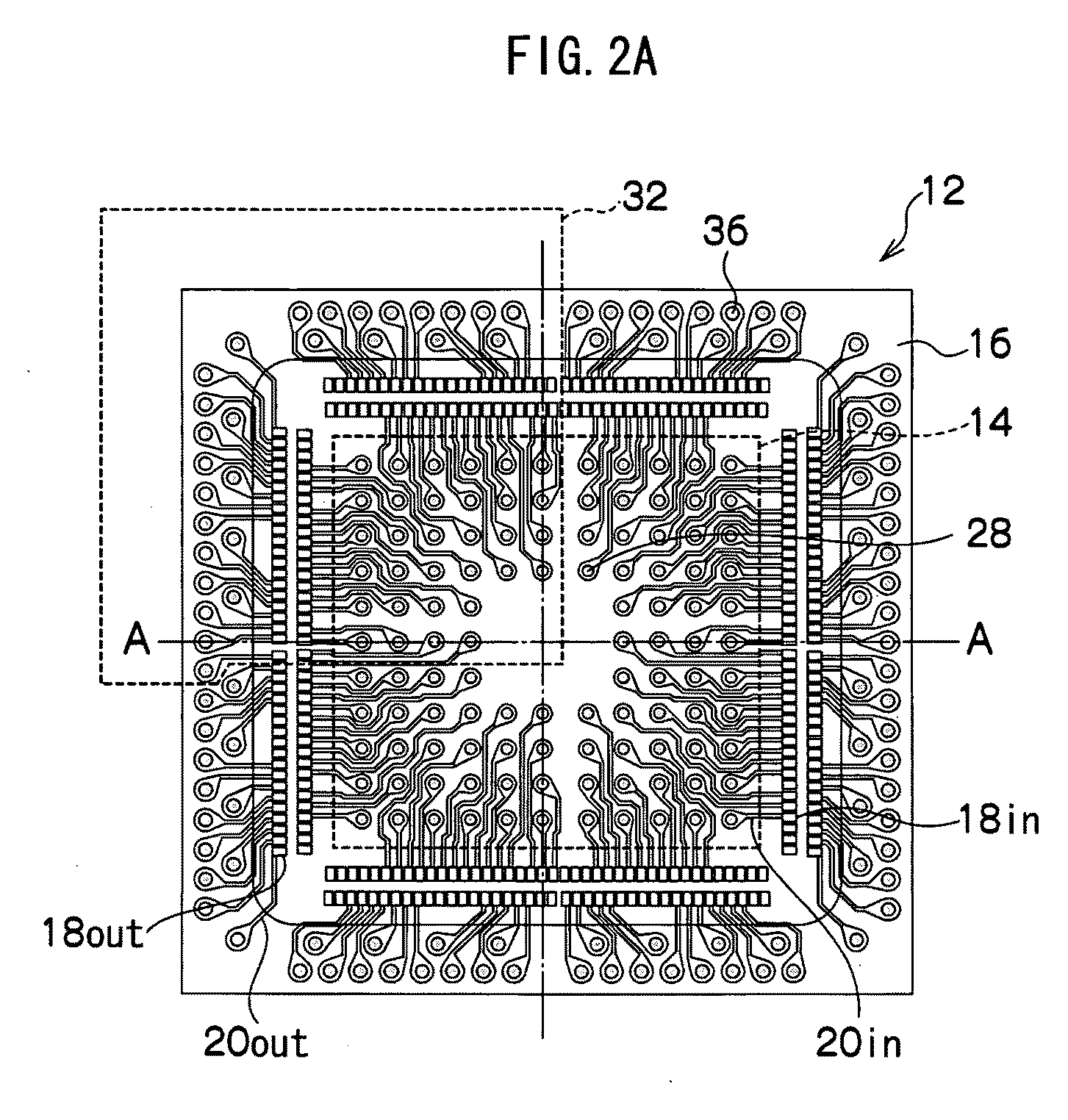
[0053]FIG. 1 is a schematic cross-sectional view illustrating a structure of the double-sided electrode package to be manufactured in the first exemplary embodiment of the invention. The double-sided electrode package 10 has a flat-plate type core material 16 composed of an insulator such as resin or ceramics. Plural via...

second exemplary embodiment

[0119]A second exemplary embodiment describes a method for manufacturing the double-sided electrode package in which semiconductor chips are mounted to a package substrate formed with plural surface-side terminals having plural protruded rims formed on entire peripheries of their side surfaces in a peripheral direction and the semiconductor chips are sealed by the liquid resin similarly to the first exemplary embodiment. In the second exemplary embodiment, the substrate frame on which plural package substrates is formed is used, and a “partitioning member” which holds back the liquid resin is formed on each package substrate on the substrate frame. After the semiconductor chips are arranged, the substrate frame is divided (separated) to form the individual package substrates. After the separation, resin sealing is carried out on each package substrate, so that the structure of the double-sided electrode package is formed. These manufacturing steps are described.

[Double-Sided Electro...

third exemplary embodiment

[0138]A third exemplary embodiment describes a method for manufacturing a double-sided electrode package where the semiconductor chips are mounted to the package substrate formed with the plural surface-side terminals having the plural protruded rims formed on the entire peripheries of their side surface in the peripheral direction, and the semiconductor chips are sealed by the liquid resin. In the third exemplary embodiment, the substrate frame formed with the plural package substrates is used, and after the double-sided electrode package structure is formed on the substrate frame, the substrate frame is divided (separated) into the individual double-sided electrode packages structures. These manufacturing steps are described. A difference from the first exemplary embodiment is that the spread of the liquid resin is controlled by not using a resin dam at the “step of sealing the semiconductor chips” but by surface tension of the liquid resin.

[Double-Sided Electrode Package]

[0139]FI...


PUM


Abstract

In a double-sided electrode package, a sealing resin layer is formed so as to fill peripheries of surface-side terminals formed on a package substrate. Since the side surfaces of the surface-side terminals have plural protruded rims, adhesion with the sealing resin layer is improved by an anchor effect. At a sealing step, since supplied liquid resin is naturally flowed to form the sealing resin layer, a “mold step” and a “grinding step” may be omitted, and thus the sealing step may be simplified more greatly than a case where the resin sealing is carried out by a transfer molding method.

Description

CROSS-REFERENCE TO RELATED APPLICATION[0001]This application claims priority under 35 USC 119 from Japanese Patent Application No. 2008-109176, the disclosure of which is incorporated by reference herein.BACKGROUND OF THE INVENTION[0002]1. Field of the Invention[0003]The present invention relates to a method for manufacturing semiconductor device. The invention particularly relates to the method for manufacturing semiconductor device having a double-sided electrode structure (double-sided electrode package).[0004]2. Description of the Related Art[0005]Recently, three-dimensional package techniques with higher packaging density are being developed according to miniaturization of electronic devices such as mobile telephones. In the three-dimensional package techniques, a package-on-package (POP) method for laminating another package on one package is one of promising candidates. In POP, lamination of multi-layered packages having three or four layers is also proposed (see Japanese Pat...

Claims


Application Information

Patent Timeline
Patent Type & Authority Applications(United States)
IPC IPC(8): H01L21/56
CPCH01L21/4846H01L2924/3511H01L23/3128H01L23/49811H01L23/49827H01L24/19H01L24/97H01L25/105H01L2224/32225H01L2224/48091H01L2224/48227H01L2224/73265H01L2224/97H01L2924/01002H01L2924/01027H01L2924/01029H01L2924/01079H01L2924/01082H01L2924/14H01L21/561H01L2924/01033H01L2924/01006H01L2924/01005H01L24/48H01L2924/07802H01L2225/1058H01L2225/1023H01L2224/83H01L2224/85H01L2924/00014H01L2924/00H01L2924/00012H01L24/45H01L24/73H01L2224/451H01L2224/45144H01L2924/181
Inventor INO, YOSHIHIKO
Owner LAPIS SEMICON CO LTD
Why Eureka
Try Eureka