Network signal coupling circuit assembly

a network signal and coupling circuit technology, applied in the field of network technology, can solve the problems of low fabrication efficiency of this kind of network connector, inseparable relationship between people and networks, and ineffective removal of noise from network signals, so as to achieve the effect of eliminating noise from network signals

Active Publication Date: 2015-10-22
AJOHO ENTERPRISE
View PDF1 Cites 5 Cited by
  • Summary
  • Abstract
  • Description
  • Claims
  • Application Information

AI Technical Summary

Benefits of technology

[0009]The present invention has been accomplished under the circumstances in view. According to one aspect of the present invention, the network signal coupling circuit assembly comprises a circuit board, a network-on-chip installed in the circuit board, a network connector, and a signal coupling circuit electrically coupled between the network-on-chip and the network connector, wherein the network-on-chip is a current-mode design; the signal coupling circuit comprises opposing first connection end and second connection end, multiple two-wire channels coupled between the first connection end and the second connection end, and a plurality of coupling modules respectively installed in the two-wire channels and respectively electrically coupled between the first connection end and the second connection end. Further, each two-wire channel consists of two wires. Each coupling module comprises a first capacitor connected to each wire. Subject to the characteristic that increasing the signal frequency can relatively increases the signal coupling strength of the capacitors, the signal coupling performance of the signal coupling circuit can be relatively enhanced if the network frequency is getting higher.
[0010]According to another aspect of the present invention, the network-on-chip is a voltage-mode design. Subject to the characteristics of the first capacitors of the coupling modules, supplying a voltage to the first end of each first capacitor can cause the first end of the respective first capacitor to generate a transient unipolar charge and the opposing second end of the respective first capacitor to generate another transient unipolar charge. When the supplied voltage is stopped after a predetermined period of time, the second end of the respective first capacitor of each coupling module discharges the negative charge through the wires of the respective two-wire channel, achieving signal coupling transmission. Further, the first capacitors can also provide an isolation effect to prohibit the signal from passing through the wires of the respective two-wire channel directly, preventing reverse current.
[0012]According to still another aspect of the present invention, the signal coupling circuit can be configured to provide a plurality of coupling modules respectively installed in the two-wire channels and respectively electrically coupled between the first connection end and the second connection end, and a plurality of filter modules respectively installed in the two-wire channels and respectively electrically coupled between and the respective coupling modules and the first connection end or second connection end. In one embodiment of the invention, each filter module comprises an inductor electrically connected in series to each wire of the respective two-wire channel. In another embodiment of the invention, each filter module comprises two second capacitors electrically connected in series between the two wires of the respective two-wire channel with the midpoint between the two second capacitors electrically connected to a second grounding terminal. By means of the inductors or second capacitors, the filter modules can effectively remove noises from the network signal.

Problems solved by technology

The development of computer technology makes the relationship between people and network unshakable and inseparable.
As shown in FIG. 7, a conventional network signal coupling assembly comprises a circuit board A, and multiple transformer coils B and Filter coils C installed in the circuit board A. Each of the transformer coils B and filter coils C comprises a wire core D, and a lead wire D1 wound round the wire core D with the ends thereof bonded to respective contacts at the circuit board A. Because the winding of the transformer coils B and the filter coils C cannot be achieved by an automatic machine and must be done by labor, the fabrication efficiency of this kind of network connector is low.
Further, the lead wire may be broken easily during winding, thereby increasing the cost.
Further, fabrication by labor cannot accurately control the coil winding tightness and number of turns, affecting product quality stability.
However, the increase of inductive reactance causes the increase of signal attenuation, leading to network disconnection or dramatic slowdown in network transmission speed.
When being over this range, the insertion loss will increase rapidly.

Method used


Image

  • Network signal coupling circuit assembly
  • Network signal coupling circuit assembly
  • Network signal coupling circuit assembly

Examples


Embodiment Construction

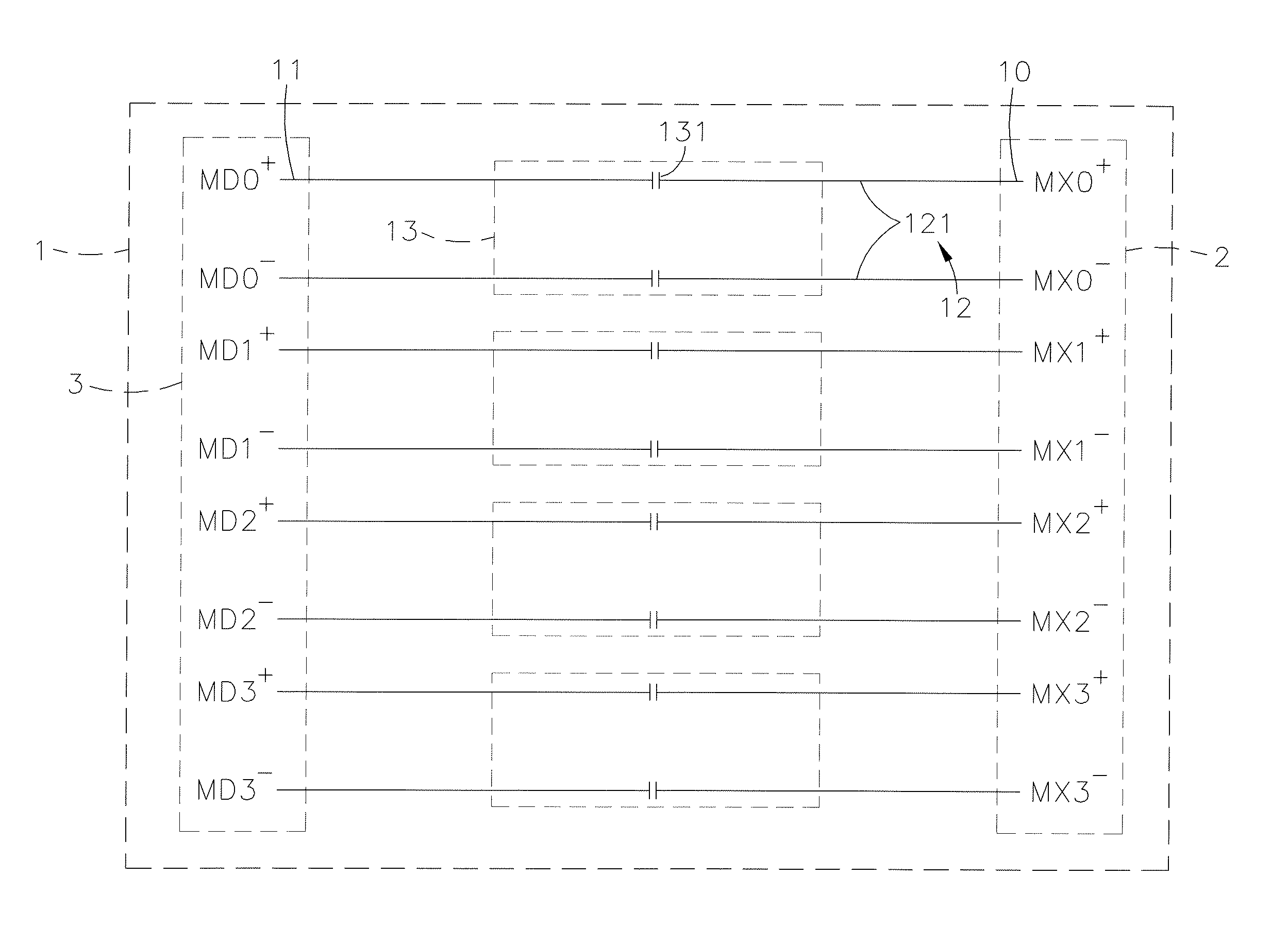
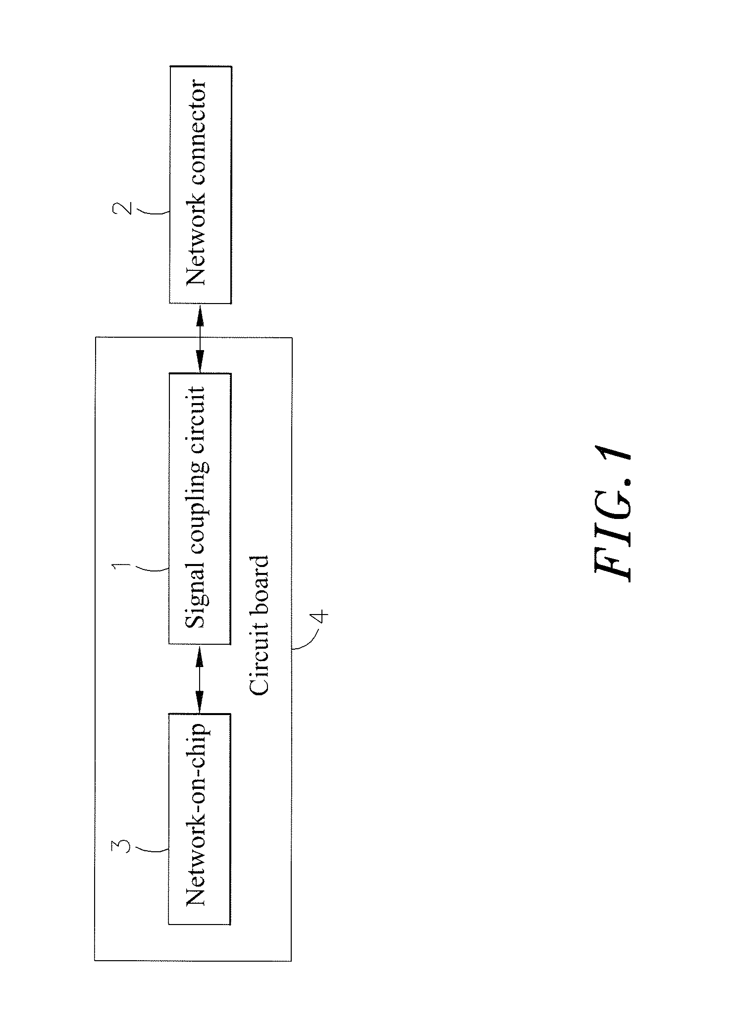
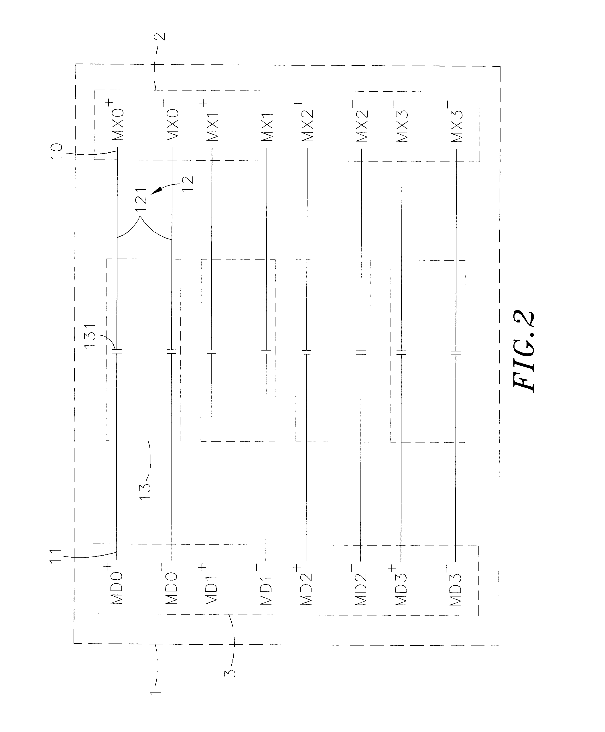
[0020]Referring to FIGS. 1 and 2, a simple circuit block diagram and a simple circuit diagram of a network signal coupling circuit assembly in accordance with the present invention are shown. As illustrated, the network signal coupling circuit assembly comprises a signal coupling circuit 1 installed in a circuit board 4 and having a first connection end 10 thereof electrically connected to a network connector 2 and an opposing second connection end 11 thereof electrically connected to a network-on-chip 3. The network-on-chip 3 is a current-mode design, and therefore, the network-on-chip 3 outputs electric current to the signal coupling circuit 1. The signal coupling circuit 1 comprises a plurality of two-wire channels 12 electrically connected in parallel between the first connection end 10 and the second connection end 11, and a plurality of coupling modules 13 respectively installed in the two-wire channels 12 and respectively electrically coupled between the first connection end ...


PUM


Abstract

A network signal coupling circuit installed in a circuit board and coupled between a network-on-chip and a network connector is disclosed to include a coupling module including a first capacitor connected in series to each wire of one respective two-wire channel of the signal coupling circuit thereof for coupling network signals and removing noises. Subject to the capacitance reactance characteristic that the signal attenuation is reduced when the frequency rises and the capacitive coupling characteristic that the signal coupling performance is enhanced when the frequency rises, the network signal coupling circuit assembly is practical for high frequency network applications to enhance signal coupling and transmission performance.

Description

CROSS-REFERENCE TO RELATED APPLICATIONS[0001]This application is a Continuation of co-pending application Ser. No. 13 / 893,962, filed on May 14, 2013, which is a Continuation-in-Part of application Ser. No. 13 / 544,538, filed on Jul. 9, 2012, which issued as U.S. Pat. No. 8,878,628 on Nov. 4, 2014, and this application is a Continuation of co-pending application Ser. No. 13 / 907,413, filed on May 31, 2013, which is also a Continuation-in-Part of application Ser. No. 13 / 544,538, filed on Jul. 9, 2012, which issued as U.S. Pat. No. 8,878,628 on Nov. 4, 2014, for which priority is claimed under 35 U.S.C. §120, and this application claims priority of Application No. 102202379 filed in Taiwan on Feb. 4, 2013, Application No. 102202378 filed in Taiwan on Feb. 4, 2013, and Application No. 101112238 filed in Taiwan on Apr. 6, 2012, under 35 U.S.C. §119; the entire contents of all of which are hereby incorporated by reference.BACKGROUND OF THE INVENTION[0002]1. Field of the Invention[0003]The p...

Claims


Application Information

Patent Timeline
Patent Type & Authority Applications(United States)
IPC IPC(8): H04L25/08H04L12/933H04L25/02
CPCH04L25/085H04L49/109H04L25/0272H04L25/0266H05K1/0233H05K1/0245H03H7/00
Inventor MO, CHIA-PINGLIU, YOU-CHI
Owner AJOHO ENTERPRISE
Why Eureka
Try Eureka