
Sic single crystal, sic wafer, sic substrate, and sic device

a technology of sic wafers and substrates, applied in the direction of crystal growth process, polycrystalline material growth, chemically reactive gases, etc., can solve the problem of difficult to convert parallel to an offset direction of the substrate into edge dislocations, affecting device characteristics, etc., to and suppress the degradation of characteristics due to a specific dislocation type

Active Publication Date: 2015-10-29
TOYOTA CENT RES & DEV LAB INC +2
View PDF2 Cites 2 Cited by
  • Summary
  • Abstract
  • Description
  • Claims
  • Application Information

AI Technical Summary

Benefits of technology

This patent relates to improving the quality of SiC single crystals and using them to create SiC devices with better performance. By optimizing the shape and growth conditions of the seed crystal, researchers have been able to produce SiC single crystals with a specific dislocation type unevenly distributed in a specific region. By cutting the SiC substrate from this specific crystal and optimizing the cutting position and size, researchers have been able to create substrates with a specific dislocation type present in a small amount. Using these substrates, researchers have been able to create SiC devices with improved performance. Overall, this patent aims to provide a better understanding and control of SiC crystals to create better SiC devices.

Problems solved by technology

However, existing SiC contains many dislocations, which greatly affect device characteristics, compared with Si.
There has been reported influence of each dislocation type on a device, such as an increase in leakage current caused by a threading dislocation such as a screw dislocation and an edge dislocation, and forward degradation of a bipolar device caused by a basal plane dislocation.
Such an attempt, however, has not achieved conversion of all basal plane dislocations into edge dislocations.
A plurality of Burgers vector directions exist in the basal plane dislocations, and a basal plane dislocation having a Burgers vector parallel to an offset direction of the substrate is difficult to be converted into edge dislocation.
However, a specific technique where a SiC single crystal is grown so as to mainly contain a specific dislocation type, or a specific technique where a SiC single crystal is grown so as to exclusively contain a specific Burgers vector has not been known.

Method used


Image

  • Sic single crystal, sic wafer, sic substrate, and sic device
  • Sic single crystal, sic wafer, sic substrate, and sic device
  • Sic single crystal, sic wafer, sic substrate, and sic device

Examples


example

Example 1

1. Sample Preparation

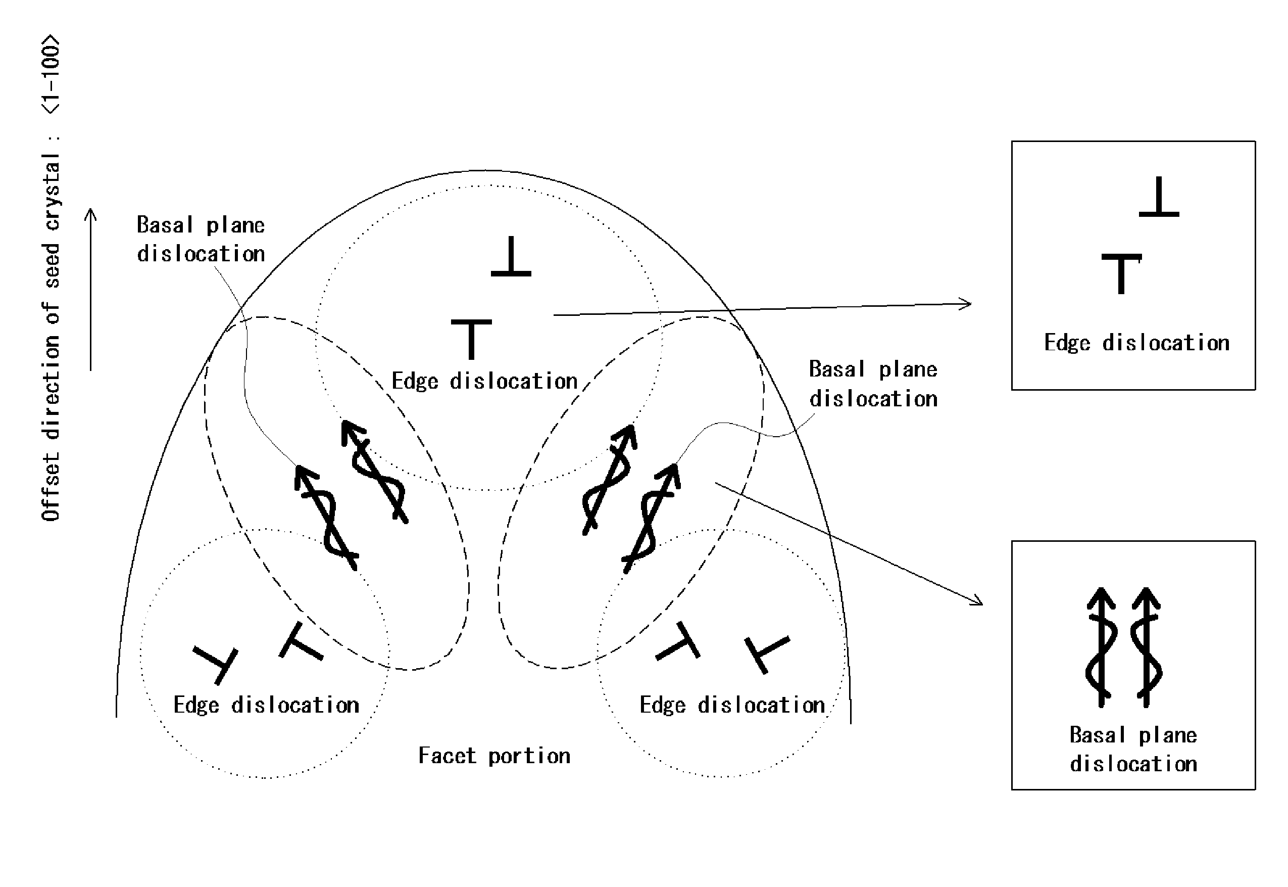
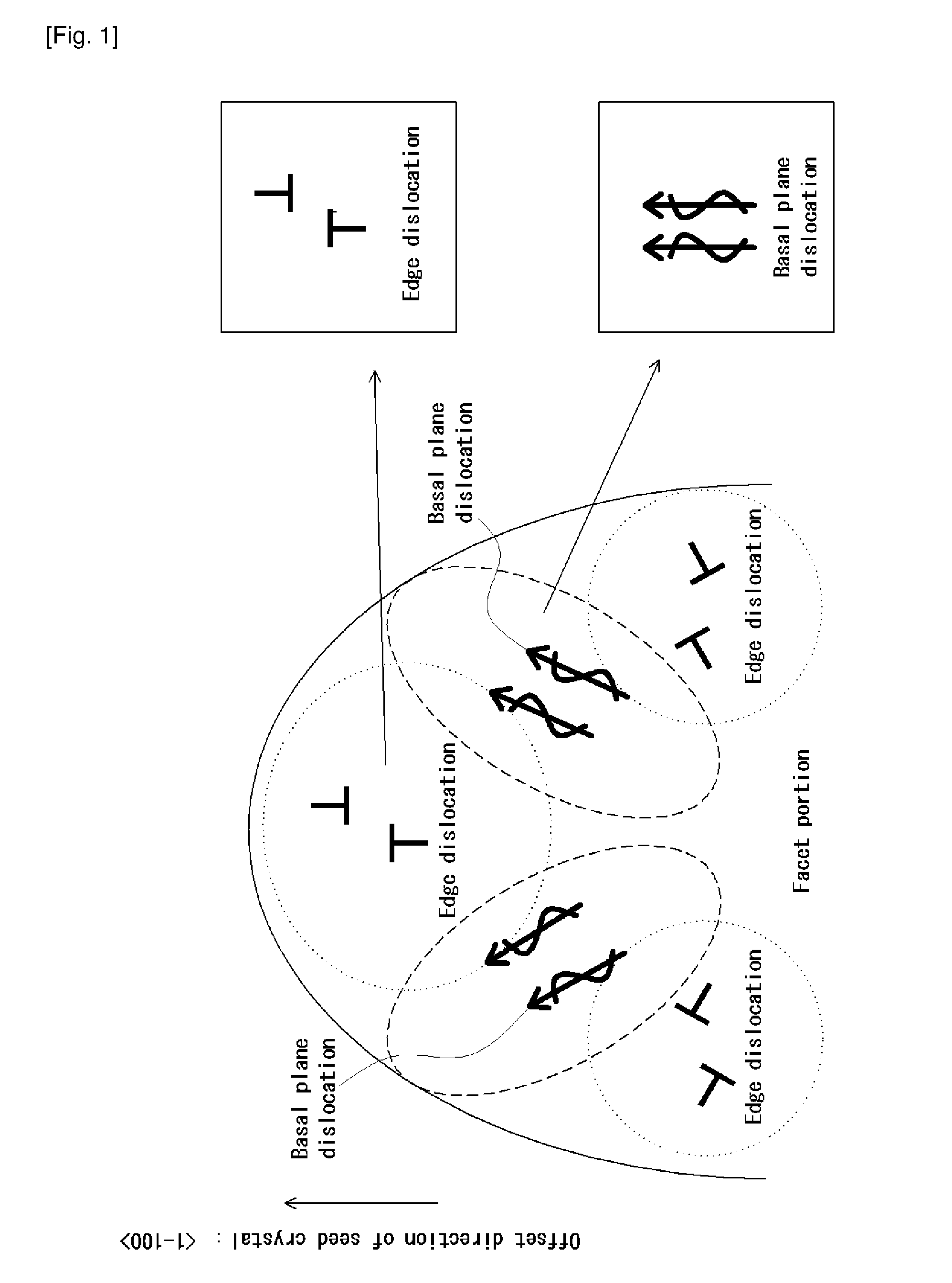
[0134]A seed crystal for c-plane growth, of which the offset direction was a direction, was cut from a crystal that was formed by repeating a-plane growth five times while a growth direction was changed. Subsequently, the surface of the seed crystal was processed such that a growth plane was configured of three planes, and an angle defined by a ridge line between the planes and a {0001} plane was 2.7 degrees.

[0135]Furthermore, a screw dislocation formable region that allowed formation of a screw dislocation was formed near an intersection between the three planes.

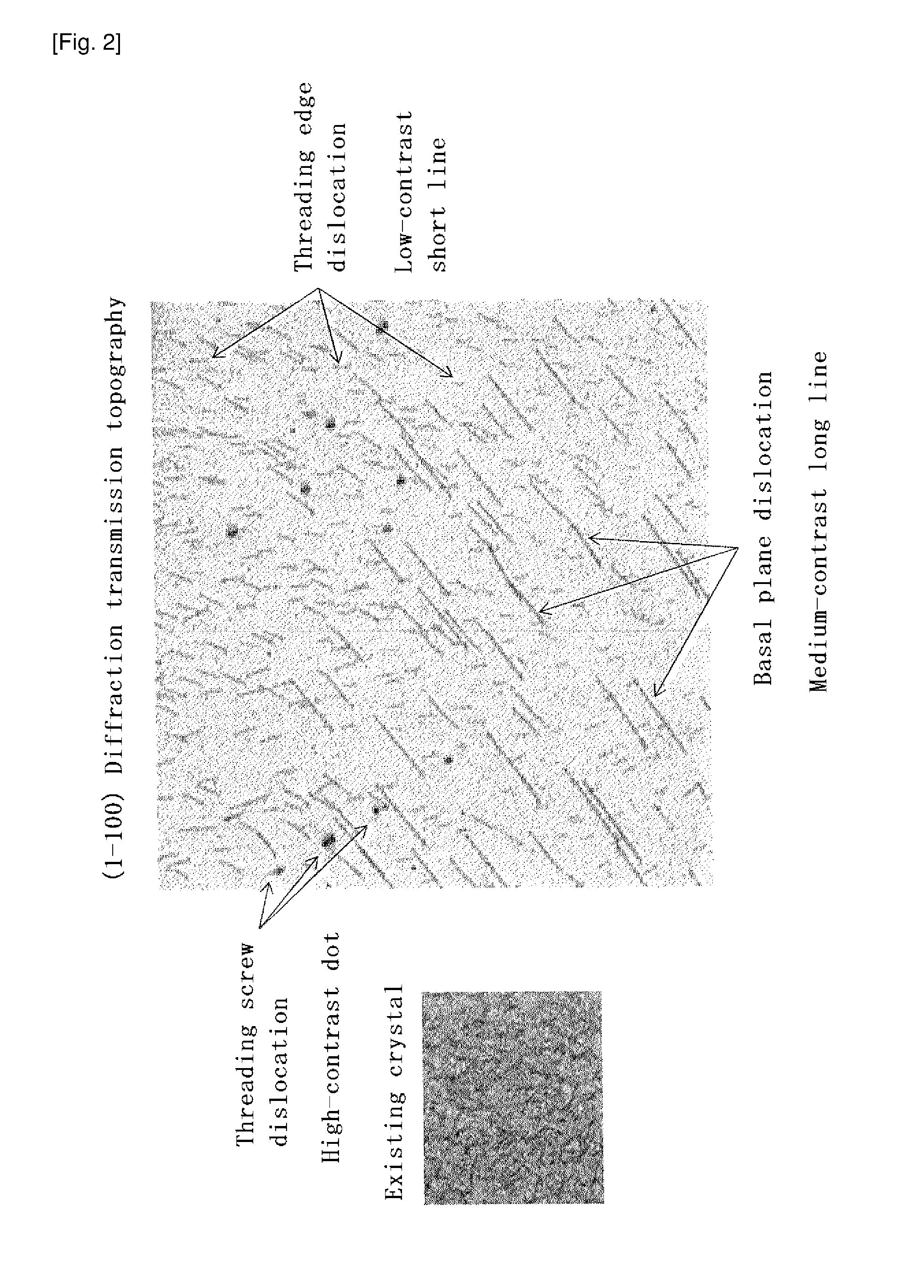
[0136]A SiC single crystal was grown by the sublimation-reprecipitation process using the resultant seed crystal. The growth was performed while a highest point of the {0001} plane, which was formed by the three planes within the screw dislocation formable region, was disposed close to the center of a crucible such that the neighborhood of the highest point of the {0001} plane was maintained a...

example 2

1. Sample Preparation

[0168]A seed crystal for c-plane growth, of which the offset direction was a direction, was cut from a crystal that was formed by repeating a-plane growth five times while a growth direction was changed. Subsequently, a surface of the seed crystal was processed such that a growth plane was configured of three planes, and an angle defined by a ridge line between the planes and a {0001} plane was 2.7 degrees.

[0169]Furthermore, a screw dislocation formable region that allowed formation of a screw dislocation was formed near an intersection between the three planes.

[0170]A SiC single crystal was grown by the sublimation-reprecipitation process using the resultant seed crystal. The growth was performed while a highest point of a {0001} plane, which was formed by the three planes within the screw dislocation formable region, was disposed close to the center of a crucible such that the neighborhood of the highest point of the {0001} plane was maintained at lowest temp...

example 3

1. Sample Preparation

[0172]A seed crystal for onset c-plane growth (the seed crystal had an onset bottom face) was cut from a crystal that was formed by repeating a-plane growth five times while a growth direction was changed. Subsequently, a surface of the seed crystal was processed such that a growth plane was configured of three planes, and an angle defined by a ridge line between the planes and a {0001} plane was 2.7 degrees. Furthermore, a screw dislocation formable region that allowed formation of a screw dislocation was formed near an intersection between the three planes.

[0173]A SiC single crystal was grown by the sublimation-reprecipitation process using the resultant seed crystal. In growth using an onset substrate, size of a facet is particularly easily increased during growth. Thus, to suppress this, the growth was performed while a site (near the center) of a seed-crystal holding base, which corresponded to the neighborhood of a highest point of the {0001} plane formed ...


PUM


Abstract

A SiC single crystal includes, in a plane substantially parallel to a c-plane thereof, a region (A) in which edge dislocations having a Burgers vector (A) in a specific direction are unevenly distributed, and a region (B) in which basal plane dislocations having a Burgers vector (B) in a specific direction are unevenly distributed. The region (A) is located in a <1-100> direction with respect to a facet portion, while the region (B) is located in a <11-20> direction with respect to the facet portion. A SiC substrate is produced by cutting a SiC wafer from the SiC single crystal in a direction substantially parallel to the c-plane, and cutting the SiC substrate from the SiC wafer such that the SiC substrate mainly contains one of the region (A) and the region (B). A SiC device is fabricated using the SiC substrate.

Description

TECHNICAL FIELD[0001]The present invention relates to a SiC single crystal, a SiC wafer, a SiC substrate, and a SiC device, and particularly relates to a SiC single crystal in which a specific dislocation type unevenly exists in a specific region, a SiC wafer and a SiC substrate cut from such a SiC single crystal, and a SiC device fabricated using such a SiC wafer or SiC substrate.BACKGROUND ART[0002]SiC has been the subject of interest as a substrate material as a successor of Si for a next-generation power device. However, existing SiC contains many dislocations, which greatly affect device characteristics, compared with Si. Hence, various proposals have been made on a technique that decreases dislocations in a SiC single crystal.[0003]For example, Patent Literature 1 discloses a technique where a conical seed crystal, of which the central axis direction is within plus or minus 10 degrees from the <0001> direction and the vertical angle is 20 degrees to 90 degrees, is used i...

Claims


Application Information

Patent Timeline
IPC IPC(8): C30B29/36C30B29/64H01L29/16C30B23/02
CPCC30B29/36H01L29/1608C30B29/64C30B23/025C30B19/12C30B25/186H01L29/045H01L29/32
Inventor GUNJISHIMA, ITARUKANZAWA, YUSUKEURAKAMI, YASUSHIKOBAYASHI, MASAKAZU
Owner TOYOTA CENT RES & DEV LAB INC
Learn More