Lc composite component

a composite component and composite technology, applied in the direction of fixed capacitors, fixed capacitor details, thin/thick film capacitors, etc., can solve the problems of difficult production of downsized lc composite components, achieve the effect of preventing the reduction of the inductance of the pattern coil, reducing the inductance of the chip capacitor, and reducing the lc composite component siz

Active Publication Date: 2015-10-29
MURATA MFG CO LTD
View PDF4 Cites 22 Cited by
  • Summary
  • Abstract
  • Description
  • Claims
  • Application Information

AI Technical Summary

Benefits of technology

[0032]According to the LC composite component of the present disclosure, it is possible to downsize the LC composite component as a chip capacitive element is provided within a pattern coil. Further, as the chip capacitive element may be downsized by configuring the chip capacitive element using a dielectric layer having a higher relative permittivity than that of an insulating layer, it is possible to prevent reduction of an inductance of a pattern coil even if the chip capacitive element is disposed within the pattern coil. Therefore, it is possible to easily achieve a desired inductance even with a downsized LC composite component.

Problems solved by technology

Therefore, it can be difficult to produce downsized LC composite components.

Method used


Image

  • Lc composite component
  • Lc composite component
  • Lc composite component

Examples


first embodiment

[0054]Hereinafter, an LC composite component will be described. The LC composite component as used herein is connected to an external connecting terminal of a device utilizing high-frequency signals, and used as a filter for removing a noise.

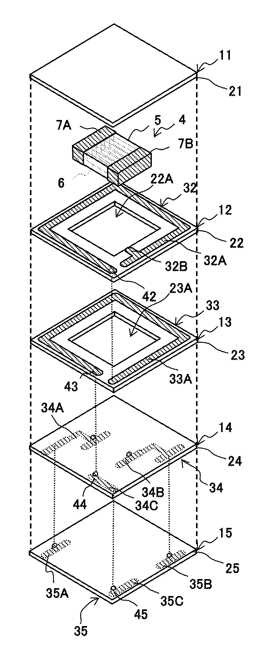
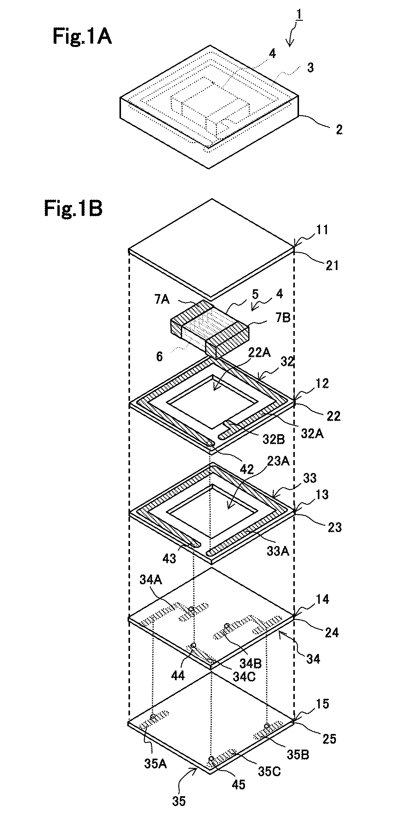
[0055]FIG. 1A is a perspective view illustrating an LC composite component 1 according to the first embodiment.

[0056]The LC composite component 1 includes a multi-layer substrate 2, a pattern coil 3, and a chip capacitive element 4. The multi-layer substrate 2 is a hexahedron, and configured herein by a thermoplastic resin such as liquid crystal polymers. The chip capacitive element 4 here is a chip capacitor. The pattern coil 3 and the chip capacitive element 4 are disposed within the multi-layer substrate 2. The multi-layer substrate may be configured by a different type of thermoplastic resin or low temperature co-fired ceramics, for example.

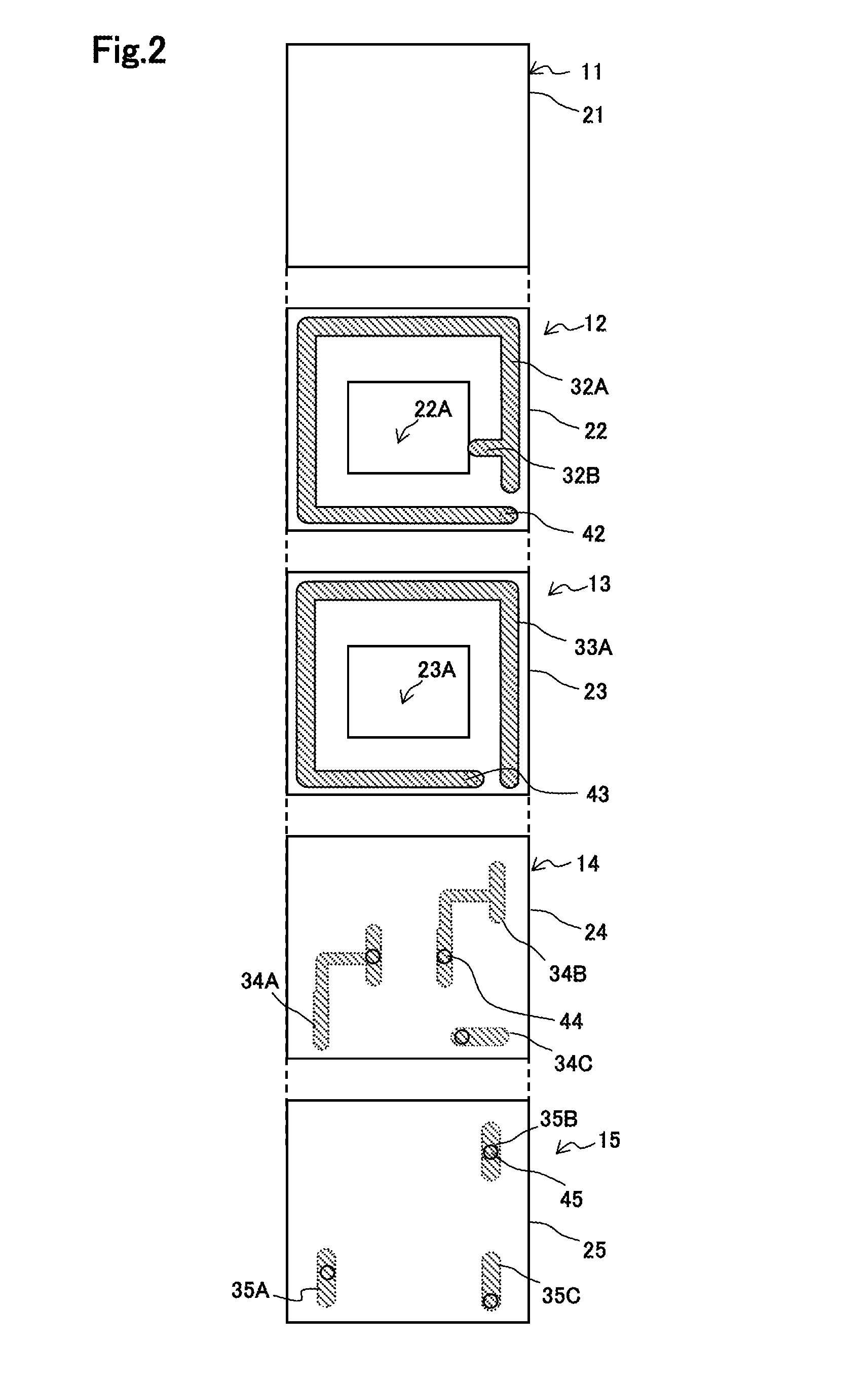
[0057]FIG. 1B is an exploded perspective view of the LC composite component 1. FIG. 2 is an exploded ...

second embodiment

[0089]Next, an LC composite component 51 according to the present disclosure will be described.

[0090]FIG. 5 is a side sectional view illustrating the LC composite component 51. FIG. 6 is an exploded plan view of the LC composite component 51 in which its layers are viewed in a planar view from their top surfaces.

[0091]The LC composite component 51 includes a multi-layer substrate 52, pattern coils 53A and 53B, and chip capacitive elements 54A and 54B. The chip capacitive elements 54A and 54B here are chip capacitors. The pattern coils 53A and 53B and the chip capacitive elements 54A and 54B are disposed within the multi-layer substrate 52.

[0092]The multi-layer substrate 52 includes insulating layers 71, 72, 73, 74, 75, 76, 77, 78, and 79. The multi-layer substrate 52 is configured such that the insulating layers 71-79 are stacked from a top surface to a bottom surface in order.

[0093]The insulating layer 71 is made of a resin, has a rectangular outline in a planar view along the stac...

third embodiment

[0114]Next, an LC composite component according to the present disclosure will be described.

[0115]FIG. 8A is a schematic view illustrating an LC composite component 101 according to the third embodiment of the present disclosure. In FIG. 8A, the pattern coil is schematically illustrated as a wire coil.

[0116]The LC composite component 101 includes a multi-layer substrate 102, pattern coils 103A and 103B, and chip capacitive elements 104A and 104B. The chip capacitive elements 104A and 104B here are chip capacitors.

[0117]The pattern coil 103A and the pattern coil 103B are in a coiled shape of which the coil axis extends along the stacking direction of the multi-layer substrate 102, and are adjacent to each other in a direction perpendicular to the stacking direction of the multi-layer substrate 102. Further, magnetic flux within the pattern coil 103A and the pattern coil 103B is directed from a bottom surface toward a top surface of the multi-layer substrate 102.

[0118]In such a config...


PUM


Abstract

Provided is an LC composite component having a multi-layer substrate, a pattern coil, and a chip capacitive element. The multi-layer substrate is configured such that insulating layers are stacked. The pattern coil forms a coiled shape of which the coil axis extends along a stacking direction of the multi-layer substrate, and includes a coil conductor disposed between the insulating layers. The chip capacitive element includes a ceramic body having a relative permittivity higher than that of the insulating layers and counter electrodes. The chip capacitive element is at least partially disposed within the pattern coil.

Description

BACKGROUND OF THE INVENTION[0001]1. Field of the Invention[0002]The present disclosure relates to an LC composite component configured such that a coil and a chip capacitive element are arranged in a multi-layer substrate having a plurality of insulating layers stacked on each other.[0003]2. Description of the Related Art[0004]There is an LC composite component that is configured as an LC filter in which a coil and a capacitor that are formed by an electrode pattern are disposed between layers in a multi-layer substrate are connected (see JP 5-335866 A).[0005]According to a conventional LC composite component, a magnetic field generated within a multi-layer substrate becomes stronger as the magnetic field is closer to a coil. Therefore, if an electrode pattern such as a capacitor is disposed near the coil, a magnetic flux travels around the electrode pattern, and thus an inductance of the coil is reduced. Accordingly, in order to set an inductance to a desired value without changing...

Claims


Application Information

Patent Timeline
Patent Type & Authority Applications(United States)
IPC IPC(8): H01G4/40H01G4/224H01G4/06H01G4/01
CPCH01G4/40H01G4/01H01G4/224H01G4/06H03H7/0107H03H7/175H03H7/1758H03H2001/0085H01F17/0013H01F27/40H01G4/33H03H7/0115H03H1/00H03H2001/0078
Inventor YOSUI, KUNIAKIBABA, TAKAHIROTAMURA, WATARU
Owner MURATA MFG CO LTD
Why Eureka
Try Eureka