Wafer processing method
- Summary
- Abstract
- Description
- Claims
- Application Information
AI Technical Summary
Benefits of technology
Problems solved by technology
Method used
Image

Examples
first embodiment
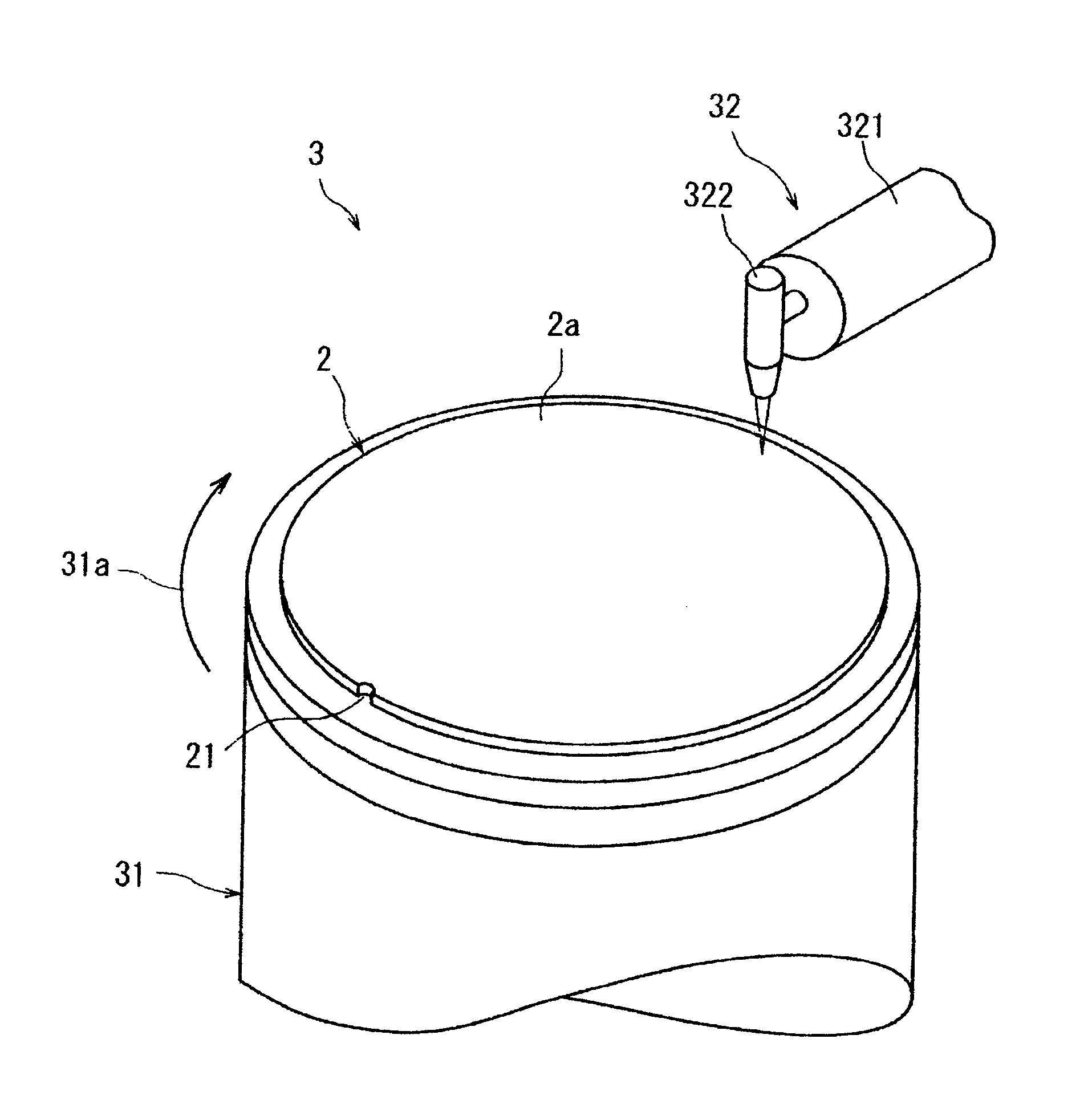
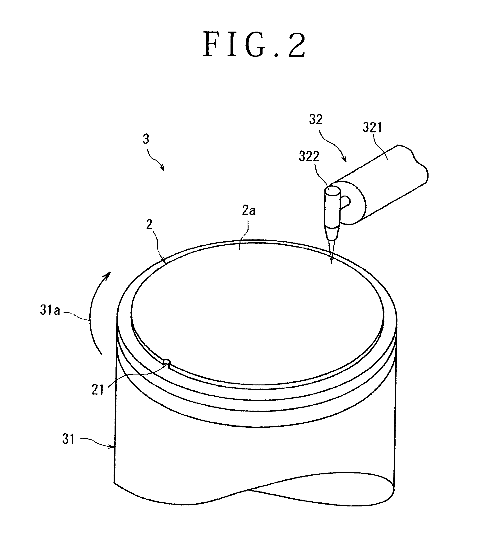
[0022]In the wafer processing method of the present invention, a crystal strain removing step of removing the crystal strains remaining in the peripheral portion of the wafer 2 is carried out. the crystal strain removing step is carried out using a laser processing apparatus 3 shown in FIG. 2. The laser processing apparatus 3 depicted in FIG. 2 includes a chuck table 31 for holding a workpiece thereon, and laser beam applying means 32 for applying a laser beam to the workpiece held on the chuck table 31. The chuck table 31 is configured to hold the workpiece by suction, and to be rotated in the direction indicated by arrow 31a in FIG. 2 by a rotating mechanism (not shown).
[0023]The laser beam applying means 32 includes a cylindrical casing 321 disposed substantially horizontally. Pulsed laser beam oscillation means (not shown) including a pulsed laser beam oscillator and repetition frequency setting means is disposed inside the casing 321. A focusing device 322 having a focusing len...
second embodiment
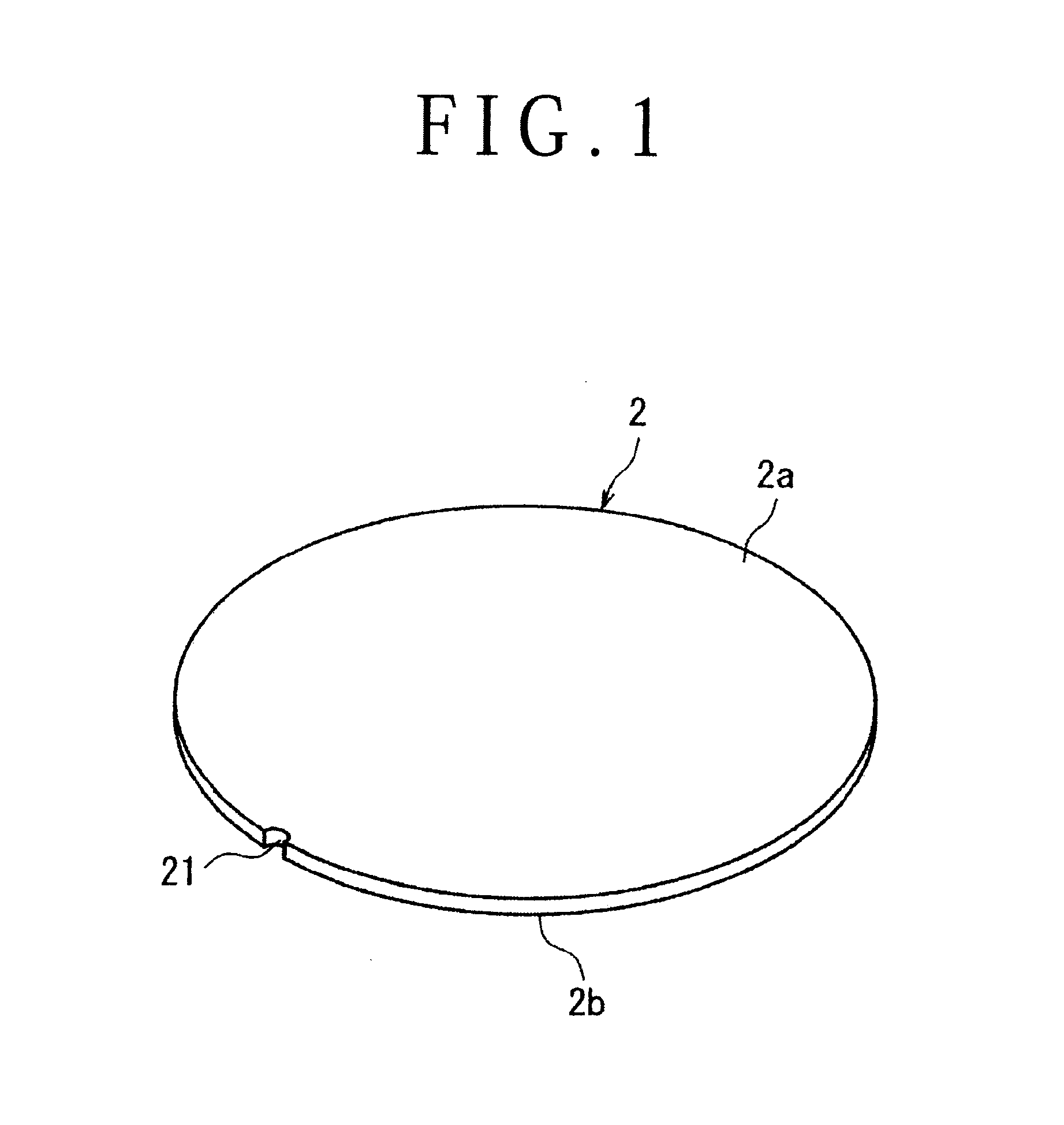
[0031]In the second embodiment, a laser beam having a wavelength such as to be absorbed in the wafer 2 is applied to the wafer 2 from one side of the wafer 2, along a line extending along the margin or the edge of the wafer 2 and spaced a predetermined distance inward from the margin, to effect ablation of the wafer 2 and form a laser-processed groove along the margin, thereby removing the peripheral wafer portion where the crystal strains are remaining. Specifically, as shown in FIGS. 6 and 7A, a position spaced a predetermined distance inward from the margin of the wafer 2 held by the chuck table 31 is positioned in a position directly under the focusing device 322. Then, while applying a pulsed laser beam having a wavelength such as to be absorbed in the wafer 2 to the wafer 2 via the focusing device 322, the chuck table 31 is rotated one revolution in the direction of arrow 31a in FIG. 7A. In this case, the focal point P of the pulsed laser beam applied via the focusing device 3...
PUM
 Abstract
Description
Claims
Application Information
PatSnap Eureka turns technology decisions into work you can execute. Powered by our Innovation Knowledge Graph, it runs expert workflows across engineering, life sciences, materials and intellectual property. Get your review-ready output in minutes.


