

Interposer and method of fabricating the same
a technology of interposers and fabrication methods, applied in the field of interposers, can solve the problems of size limitation, size limitation, and size limitation of silicon interposers from leading foundries, and achieve the effect of large room
- Summary
- Abstract
- Description
- Claims
- Application Information
AI Technical Summary
Benefits of technology
Problems solved by technology
Method used
Image

Examples
Embodiment Construction
[0017]The following description is a mode for carrying out the invention. This description is for the purpose of illustrating the general principles of the invention and should not be taken in a limiting sense. The scope of the invention is best determined by reference to the appended claims. Wherever possible, the same reference numbers are used in the drawings and the descriptions to refer to the same or like parts.
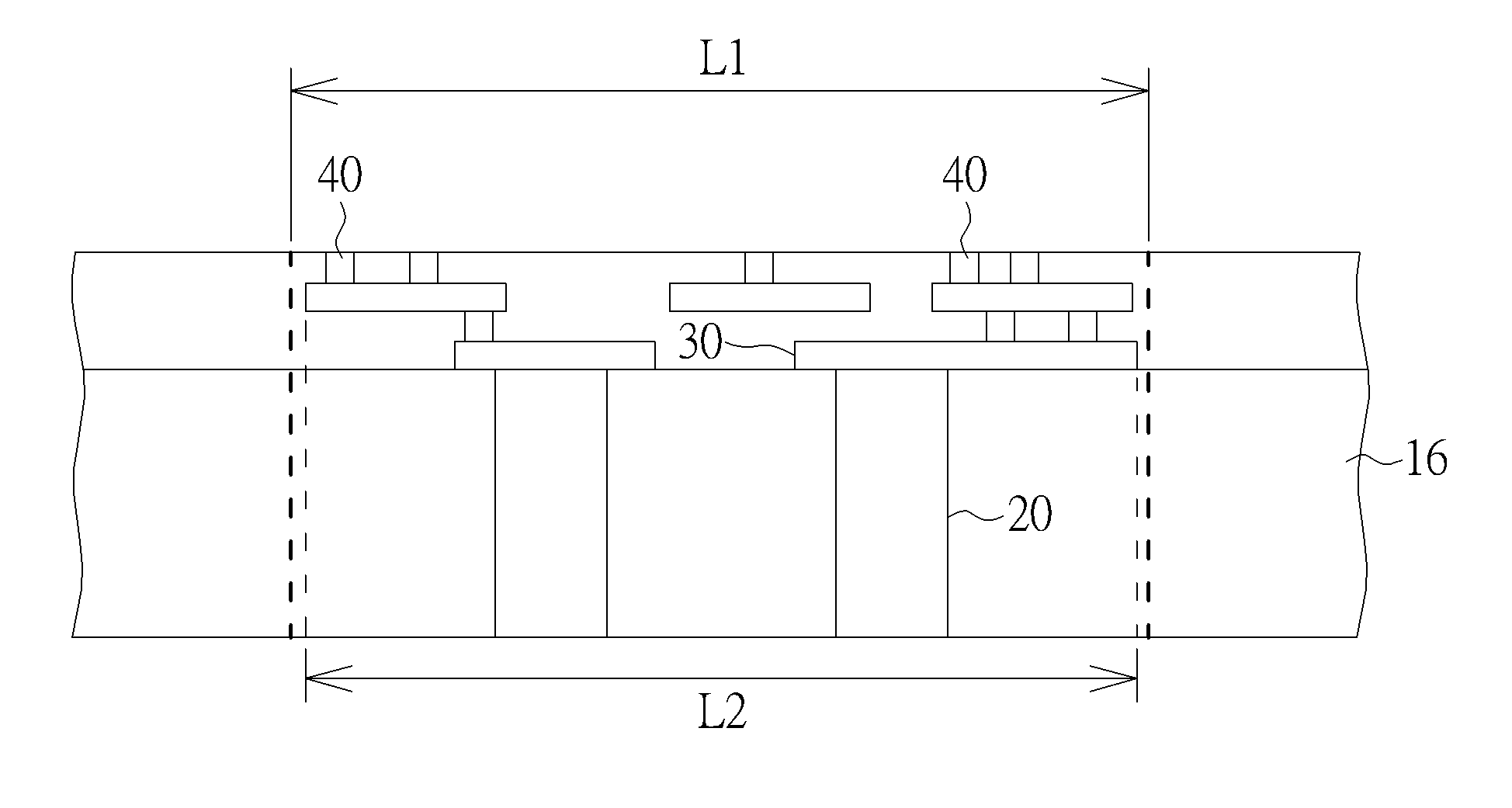
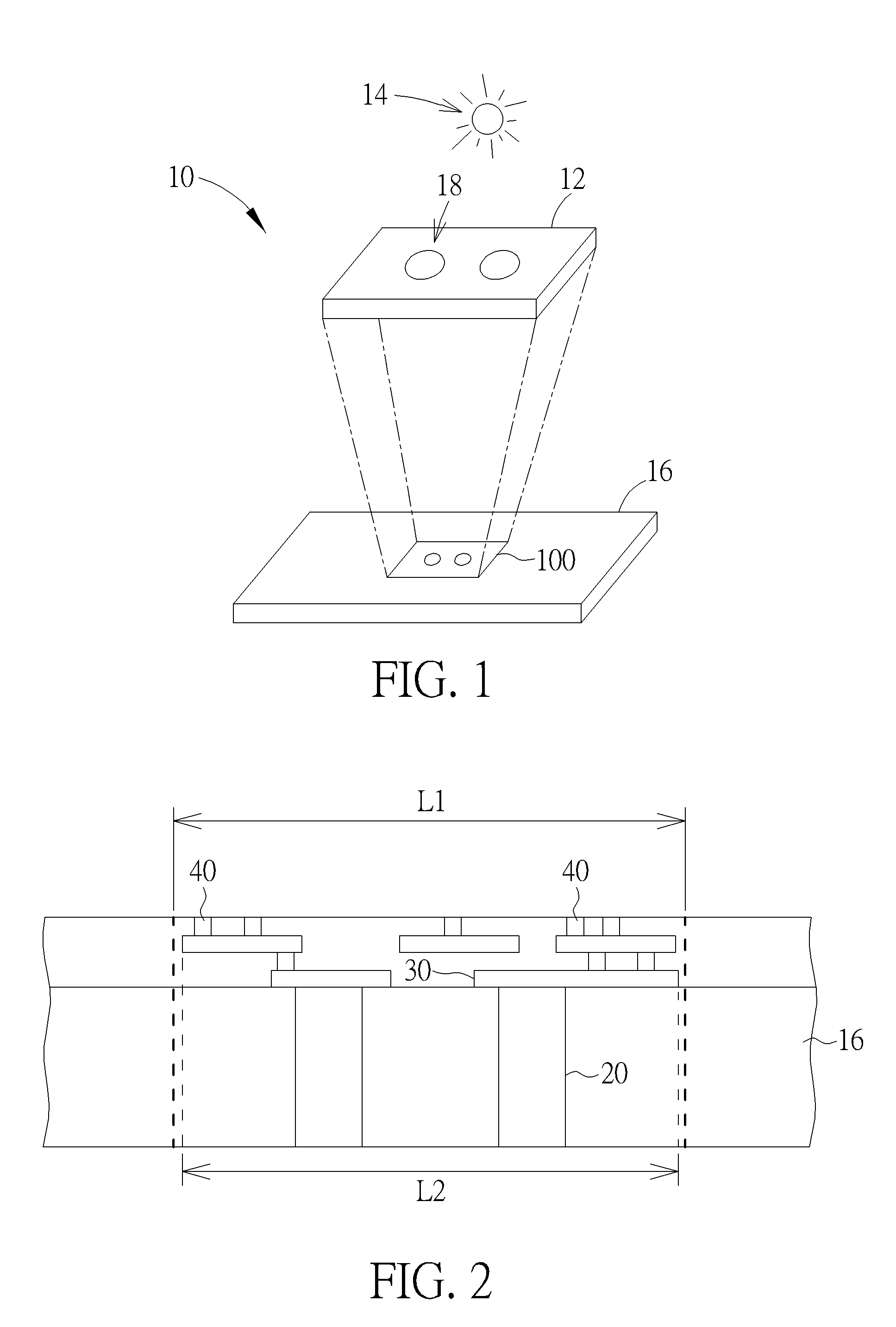
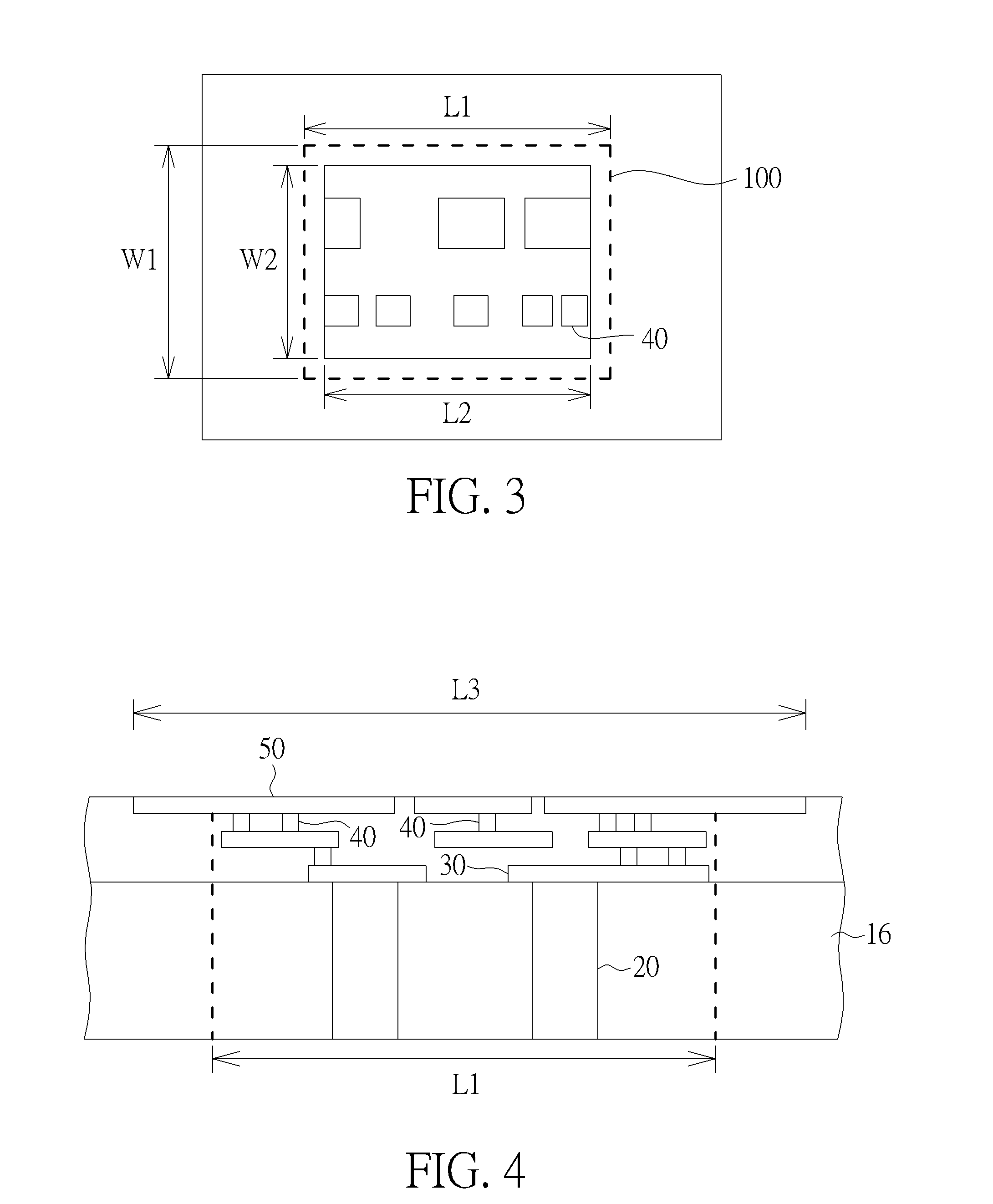
[0018]FIG. 1 to FIG. 11 schematically depict a fabricating method of a large interposer according to a preferred embodiment of the present invention, wherein like reference numerals are used to refer to like elements throughout. The implementation of the present invention is divided into two stages: firstly, several interconnection layers are formed on a substrate. The sizes of interconnection layers are all within the maximum exposure region (i.e. a maximum field which can be defined by a single shot of a lithographic scanner); and secondly, an uppermost circuit design...
PUM
| Property | Measurement | Unit |
|---|---|---|
| size | aaaaa | aaaaa |
| size | aaaaa | aaaaa |
| length | aaaaa | aaaaa |
Abstract
Description
Claims
Application Information