Optical receiving device and phase cycle reduction method

a technology of optical receiving device and phase cycle, applied in the field of communication system, can solve the problem of system conspicuous influence of phase noise, achieve the effect of reducing the frequency of phase cycle slips, improving the estimation accuracy of carrier phase estimation values, and improving detection accuracy

Active Publication Date: 2015-11-19
NIPPON TELEGRAPH & TELEPHONE CORP
View PDF5 Cites 9 Cited by
  • Summary
  • Abstract
  • Description
  • Claims
  • Application Information

AI Technical Summary

Benefits of technology

[0020]According to this invention, even if phase cycle slip does occur, by detecting and compensating this phase cycle slip in a phase cycle slip determination/compensation unit, it is possible to reduce the frequency of phase cycle slip occurrence. Furthermore, by using a gain adjustment circuit to improve the estimation accuracy of carrier phase estimation values created by the carrier phase estimation unit, it is possible to improve the ac

Problems solved by technology

In contrast, in an optical transmission system in which coherent detection is utilized, because amplitude and amplitude information are used, such a system is conspicuously affected by phase noise (i.e., noise in the phase direction).
Main sources of such phase noise inc

Method used


Image

  • Optical receiving device and phase cycle reduction method
  • Optical receiving device and phase cycle reduction method
  • Optical receiving device and phase cycle reduction method

Examples


first embodiment

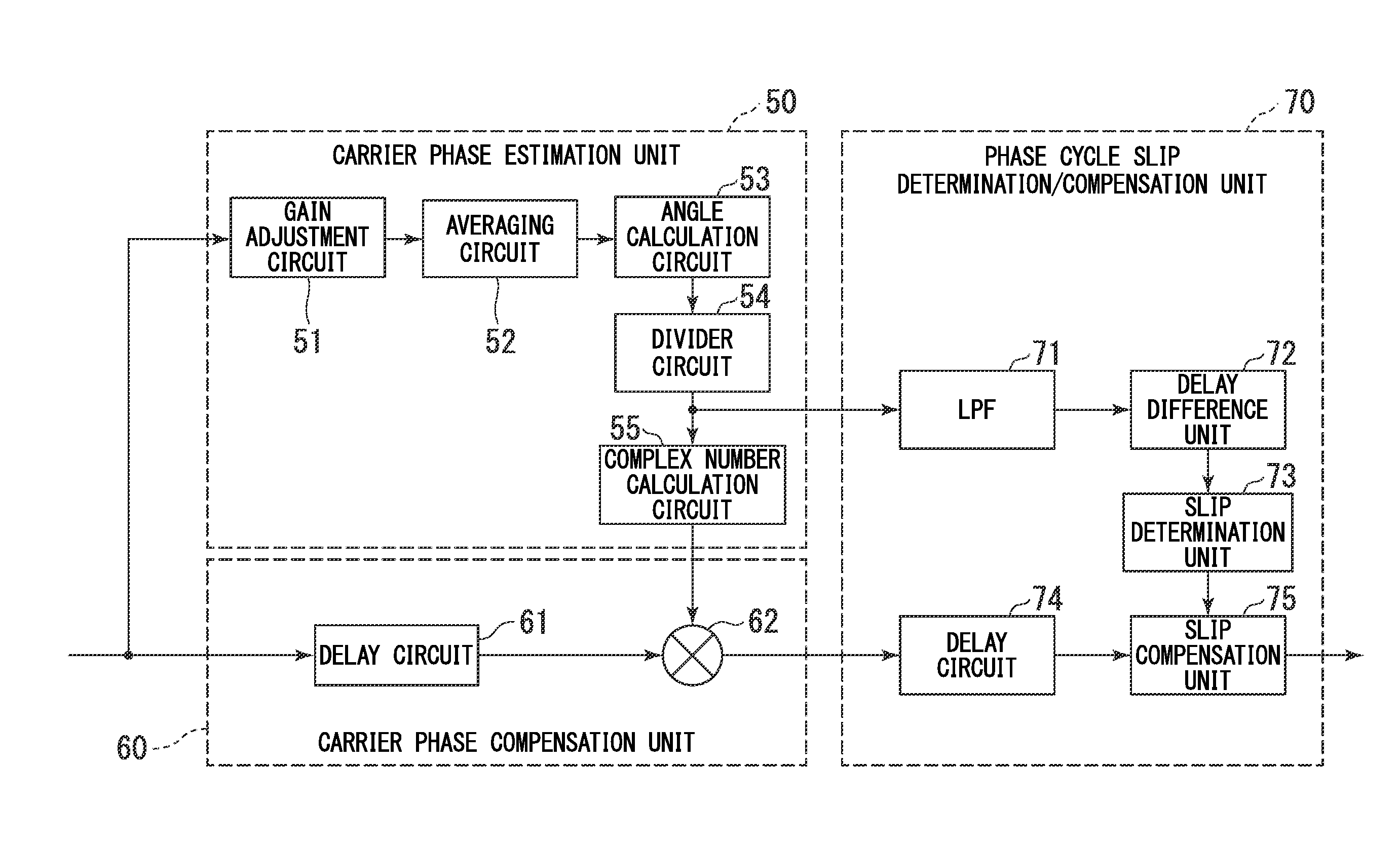
[0062]FIG. 1 is a block diagram showing the structures of a carrier phase synchronization circuit (CPR) and a phase cycle slip determination / compensation unit according to embodiments of the present invention.

[0063]Symbols input into the CPR are input into both a carrier phase estimation unit 50 and a carrier phase compensation unit 60. In the carrier phase estimation unit 50, the input symbols are input into a gain adjustment circuit 51.

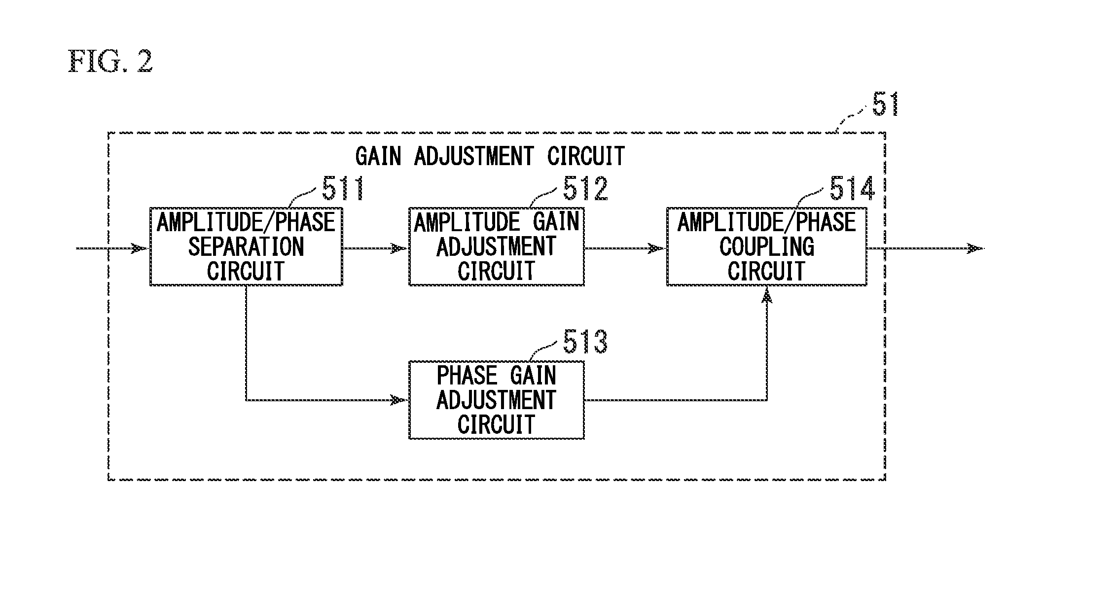
[0064]As is shown in FIG. 2, the gain adjustment circuit 51 is formed by an amplitude / phase separation circuit 511 that calculates and separates amplitude values and phase values of input symbols, an amplitude gain adjustment circuit 512 into which the amplitude values separated by the amplitude / phase separation circuit 511 are input, a phase gain adjustment circuit 513 into which the phase values separated by the amplitude / phase separation circuit 511 are input, and an amplitude / phase recombination circuit 514 that recombines the output from the am...

second embodiment

[0079]FIG. 4 is a block diagram showing an example of the structure of a receiver device according to a second embodiment. In a receiver device 80 shown in FIG. 4, the present invention is applied to a digital coherent transmission system.

[0080]Optical signals transmitted on an optical fiber transmission path are input into the receiver device 80. The receiver device 80 acquires data contained in the input optical signals, and outputs this acquired data to devices and the like that are connected downstream from it. The receiver device 80 is equipped with a local oscillator laser emitter 81, an optical 90 degree hybrid 82, a photoelectric conversion unit 83, an A / D converter 84, a wavelength dispersion compensation unit 85, an adaptive equalization unit 86, a frequency offset compensation unit 87, a phase cycle slip reduction unit 88, a phase compensation unit 89, an error correction / determination unit 90, and a client interface 91.

[0081]The optical signals input into the receiver de...

third embodiment

[0088]FIG. 5 is a block diagram showing the structure of a phase compensation circuit according to a third embodiment. In this phase compensation unit, a phase cycle slip reduction unit / carrier phase estimation unit 501 and the carrier phase compensation unit 60 correspond to the phase cycle slip reduction unit 88 shown in FIG. 4, and the phase cycle slip determination / compensation unit 70 corresponds to the phase compensation unit 89 shown in FIG. 4.

[0089]Input symbols that are input in sequence into the phase compensation circuit are input into the gain adjustment circuit 51, which is functioning as an N-power circuit (hereinafter, referred to as an N-power circuit), and the delay circuit 61. It should be noted, however, that the N-power circuit is described simply as one example of the gain adjustment circuit 51, and the present invention is not limited to this. The N-power circuit 51 raises input symbols to the N-th power. This operation to raise input symbols to the N-th power ...


PUM


Abstract

An optical receiving device receives an optical signal that has been modulated by means of phase modulation or quadrature amplitude modulation, converts the received optical signal into an electrical signal using coherent detection, and performs phase compensation on the converted received signal, and includes: a carrier phase estimation unit that estimates carrier phase errors in a received symbol string obtained from the received signal; a gain adjustment unit that performs gain adjustment on symbols input into the carrier phase adjustment unit; a phase cycle slip reduction unit that, by performing statistical processing on an output from the carrier phase estimation unit, detects general noise that causes a phase cycle slip, and reduces the phase cycle slip; and a phase compensation circuit that compensates carrier phase errors contained in the received signal using an output from the carrier phase estimation unit.

Description

TECHNICAL FIELD[0001]The present invention relates to a communication system, and to a technology that reduces the occurrence of cycle slips in a carrier synchronous circuit.[0002]Priority is claimed on Japanese Patent Applications Nos. 2013-12403, filed Jan. 25, 2013, and 2013-36126 filed Feb. 26, 2013, the contents of which are incorporated herein by reference.BACKGROUND ART[0003]In a trunk optical transmission system there is a need to store high-speed client signals economically, and transmit huge volumes of information. As part of the process to achieve this objective, from the standpoint of improving the frequency utilization efficiency, a digital coherent transmission method which employs a combination of coherent detection and digital signal processing is being investigated, and it is anticipated that it will be possible to achieve high-speed, high-volume information transmissions by means of wavelength division multiplexing using the aforementioned transmission method. In t...

Claims


Application Information

Patent Timeline
IPC IPC(8): H04B10/61H04L27/38H04L7/00H04L27/06
CPCH04B10/6165H04L27/066H04L7/0075H04L7/0041H04L27/389
Inventor HORIKOSHI, KENGOSHIBAHARA, KOHKIYAMAZAKI, ETSUSHIYOSHIDA, MITSUTERUISHIHARA, KOICHIKOBAYASHI, TAKAYUKIKISAKA, YOSHIAKIOHARA, TAKUYATOMIZAWA, MASAHITOKATAOKA, TOMOYOSHI
Owner NIPPON TELEGRAPH & TELEPHONE CORP
Why Eureka
Try Eureka