One glass solution touch panel and manufacturing method thereof and touch panel display

a glass solution and manufacturing method technology, applied in the field of crystal display technology, can solve the problems of polluting chambers, needing reverse process, and complicated production process

Active Publication Date: 2015-11-26
BOE TECH GRP CO LTD +1
View PDF6 Cites 11 Cited by
  • Summary
  • Abstract
  • Description
  • Claims
  • Application Information

AI Technical Summary

Benefits of technology

[0025]In addition, the shielding ITO layer arranged on the BM in the present disclosure may prevent the liquid crystal display (LCD) from interfering signals of the metal wirings surrounding the touch pa

Problems solved by technology

However, if directly replacing the ITO bridge 5 in the prior art with a metal bridge, there will be a problem during the preparation, that is, the metal wirings 6 need to be produced first, and then other respective layers are position aligned with the metal wirings 6.
This process will cause the metal

Method used


Image

  • One glass solution touch panel and manufacturing method thereof and touch panel display
  • One glass solution touch panel and manufacturing method thereof and touch panel display
  • One glass solution touch panel and manufacturing method thereof and touch panel display

Examples


first embodiment

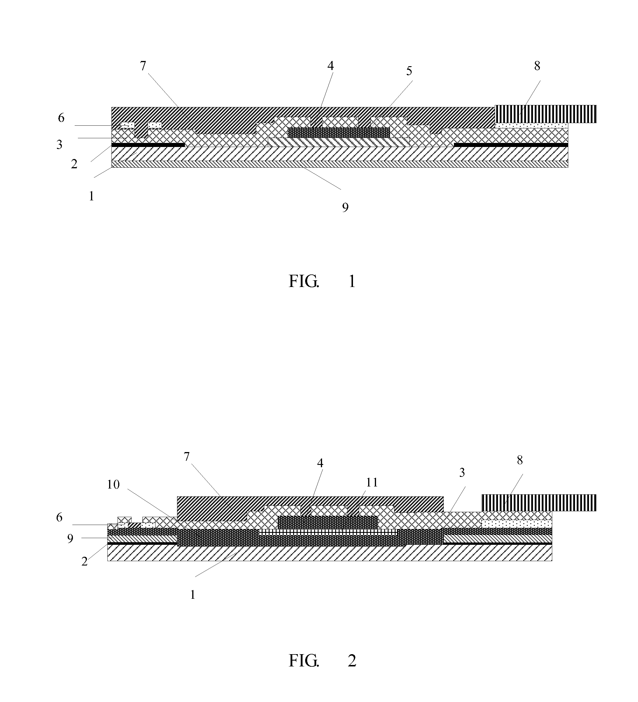
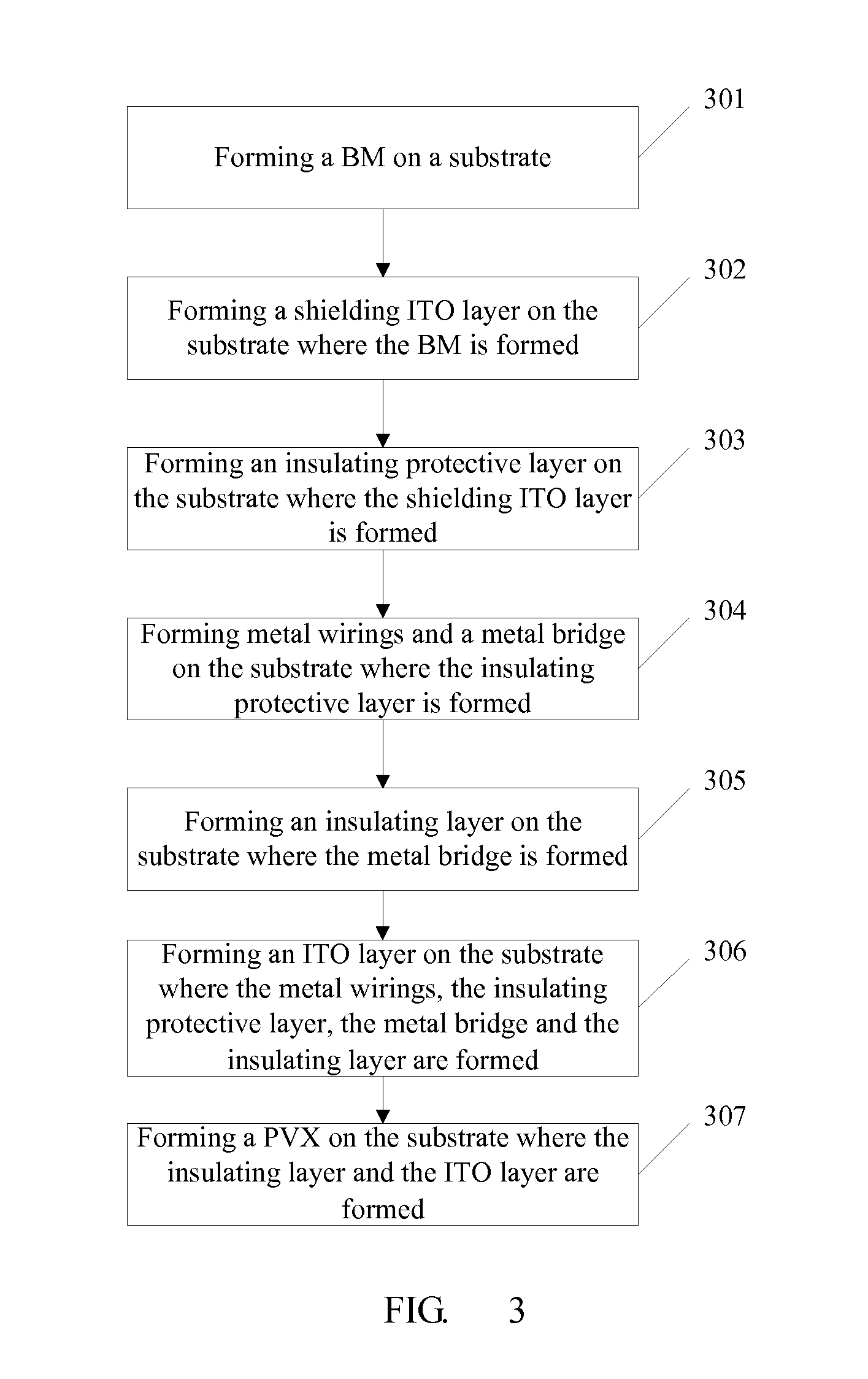
[0041]FIG. 2 is a structure schematic diagram of the one glass solution touch panel in the present invention, as shown in FIG. 2, comprising: a BM frame 2 arranged on a substrate 1, a shielding ITO layer 9 arranged on the BM frame 2, a insulating protective layer 10 arranged on the shielding ITO layer 9 and the substrate 1, metal wirings 6 and a metal bridge 11 arranged on the insulating protective layer 10, a insulating layer 4 arranged on the metal bridge 11, an ITO electrode layer 3 arranged on the metal wirings 6, the insulating protective layer 10, the metal bridge 11 and the insulating layer 4, a FPC 8 arranged on the ITO electrode layer 3, and a PVX 7 arranged on the insulating layer 4 and the ITO electrode layer 3.

[0042]Wherein, the shapes of patterns of said BM frame 2 and that of the shielding ITO layer 9 are the same; the shapes of patterns of said PVX 7 and that of the BM frame 2 are complementary to each other, or the shapes of patterns of said PVX 7 and that of the shi...

second embodiment

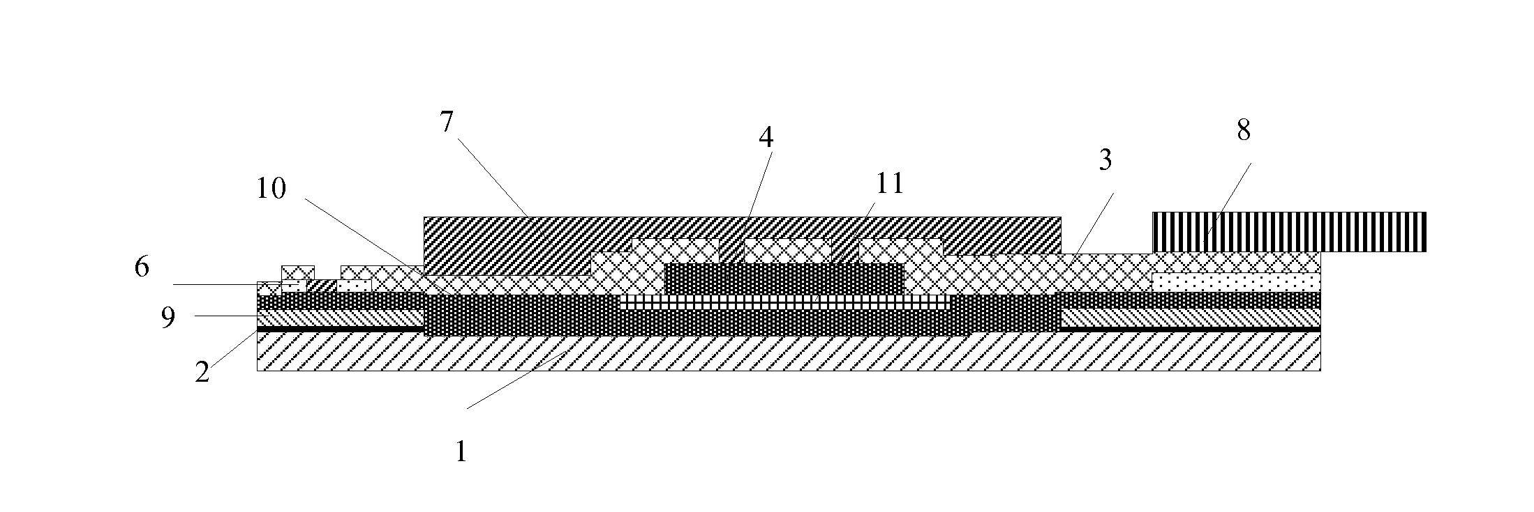
[0073]FIG. 4 is a structure schematic diagram of the one glass solution touch panel in the present invention, as shown in FIG. 4, comprising: a BM frame 2 and a metal bridge 11 arranged on a substrate 1, an insulating protective layer 10 arranged on the BM frame 2, metal wirings 6 arranged on the insulating protective layer 10, an insulating layer 4 arranged on the metal bridge 11, an ITO electrode layer 3 arranged on the substrate 1, the metal bridge 11, the insulating layer 4, the insulating protective layer 10 and the metal wirings 6, a PVX 7 arranged on the ITO electrode 3, the insulating layer 4 and the insulating protective layer 10, a shielding ITO layer 9 arranged on the PVX 7, and an FPC 8 arrange on the ITO electrode layer 3.

[0074]Wherein, the shapes of patterns of the BM frame 2 and that of the insulating protective layer 10 are the same; the shapes of patterns of the PVX 7 and that of the BM frame 2, or that of the insulating protective layer 10, are complementary to eac...


PUM

PropertyMeasurementUnit
Flexibilityaaaaaaaaaa
Shapeaaaaaaaaaa

Abstract

The present disclosure provides a one glass solution touch panel comprising a substrate, a shielding indium tin oxide layer, a black matrix frame arranged on the substrate, metal wirings arranged above the black matrix frame, a metal bridge formed in a touch sensing region, an insulating layer formed on the metal bridge, indium tin oxide electrode layers arranged on the metal wirings, the metal bridge and the insulating layer, and passivation layers arranged on the indium tine oxide electrode layers. An insulating and protecting layer is at least arranged above the black matrix frame and under the metal wirings. Meanwhile, the present disclosure further provides a method for manufacturing the one glass solution touch panel, and a touch panel display comprising the one glass solution touch panel. According to the present disclosure, the production process of the touch panel may prevent metal from sputtering the BM and ensure the chamber to be clean when other respective layers and metal wirings are in the position aligning production.

Description

TECHNICAL FIELD[0001]The embodiments of the present invention relate to crystal displaying technology, and particularly to a one glass solution touch panel and a manufacturing method thereof, and a touch panel display.BACKGROUND[0002]Currently, with the rapid development of the touch panel display, it has become a mainstream flat-panel display. From it appeared till now, the touch panel display is divided into three main types according to structures: out cell touch panel, on cell touch panel, and in cell touch panel. Currently mainstream touch panels mostly adopt the structure design with the out cell touch panel. With the continuous improvement of the optical and electrical properties required by the touch panel display as well as the continuously increasing requirement of the thinning display from customers, within a limited space, and in the case of the display effects remaining unchanged, to design a thin-film transistor with high-performance, low-cost and super-thinness has be...

Claims


Application Information

Patent Timeline
IPC IPC(8): G06F3/044H05K3/12H05K7/02
CPCG06F3/044H05K7/02Y10T29/49149G06F2203/04103G06F2203/04111H05K3/1216G06F3/0443
Inventor LIU, YINGMINGWANG, HAISHENGYANG, SHENGJIDENG, LIGUANGDUAN, YAFENG
Owner BOE TECH GRP CO LTD
Why Eureka
Try Eureka