Method for cmp of high-k metal gate structures

a metal gate and high-k technology, applied in the direction of semiconductor devices, electrical equipment, basic electric elements, etc., can solve the problems of serious affecting the performance and yield of the manufactured semiconductor device, the polysilicon gate is prone to over-polishing, and the polysilicon gate may be over-polished

Active Publication Date: 2015-11-26
SEMICON MFG INT (SHANGHAI) CORP
View PDF17 Cites 1 Cited by
  • Summary
  • Abstract
  • Description
  • Claims
  • Application Information

AI Technical Summary

Benefits of technology

[0009]Embodiments of the present invention provide a method for manufacturing a semiconductor device structure and a semiconductor device that can prevent the polysilicon gate from being over-polished while performing a CMP process on the metal gate.
[0010]In accordance with the present invention, a method for manufacturing a semiconductor device containing a front-end device with a metal gate in a metal gate transistor region and a polysilicon gate in a polysilicon gate region allows the chemical mechanical polishing of the metal gate without damaging the polysilicon gate. The method includes removing a thickness of the dummy gate in a metal gate transistor region and a polysilicon gate in a polysilicon gate transistor region and forming a protective layer on the polysilicon layer to protect the polysilicon layer during a CMP process, thereby improving the performance and yield of the semiconductor device.
[0025]In accordance with the present invention, by removing a thickness of the first dummy gate, a thickness of the second dummy gate and a thickness of the polysilicon gate so that the protective layer subsequently disposed on the first, second and polysilicon gates is below the metal gate layer, and by selecting a suitable slurry for the CMP process, an over-polishing of the polysilicon gate can be prevented, thereby improving the performance and yield of the semiconductor device. A suitable slurry may have a removal rate of the protective layer lower than a removal rate of the metal gate layer.

Problems solved by technology

Since a conventional CMP process utilizes a polish slurry that has a polysilicon removal rate greater than the aluminum removal rate, the polysilicon gate tends to be over-polished.
Furthermore, an over-polishing of the polysilicon gate may occur during the CMP process of the aluminum gate of the N-type transistors.
As can be clearly seen, the height of the polysilicon gate transistor region is significantly reduced due to over-polishing, which seriously affects the performance and yield of the manufactured semiconductor device.
Thus, the conventional CMP process of planarizing the metal gate (e.g., aluminum) uses a slurry that has a higher metal removal rate than that of the polysilicon, resulting in an over-polishing of the polysilicon gate and impacting the performance and yield of the semiconductor device.

Method used


Image

  • Method for cmp of high-k metal gate structures
  • Method for cmp of high-k metal gate structures
  • Method for cmp of high-k metal gate structures

Examples


embodiment 1

[0039]FIGS. 2A to 2F are cross-sectional views depicting stages of a method of manufacturing a semiconductor device according to an embodiment of the present invention, and FIG. 3 is a simplified flow chart of a method of manufacturing a semiconductor device according to an embodiment of the present invention. With reference to FIGS. 2A-2F and FIG. 3, a method according to the embodiment may include the following steps:

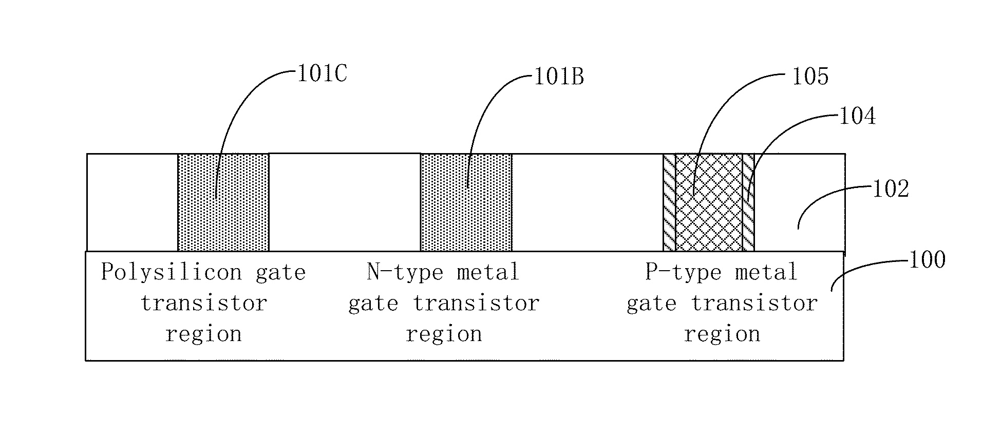
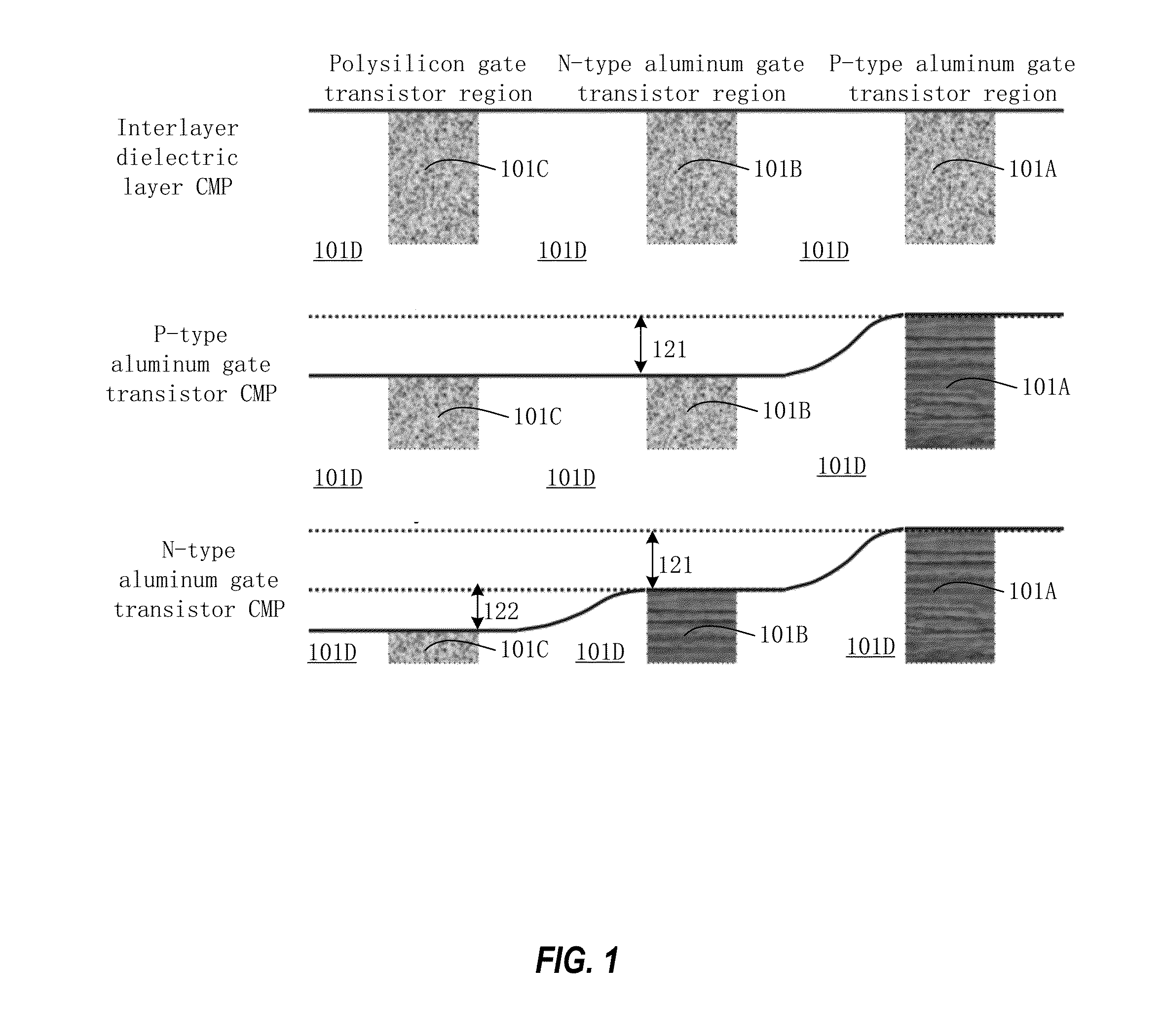
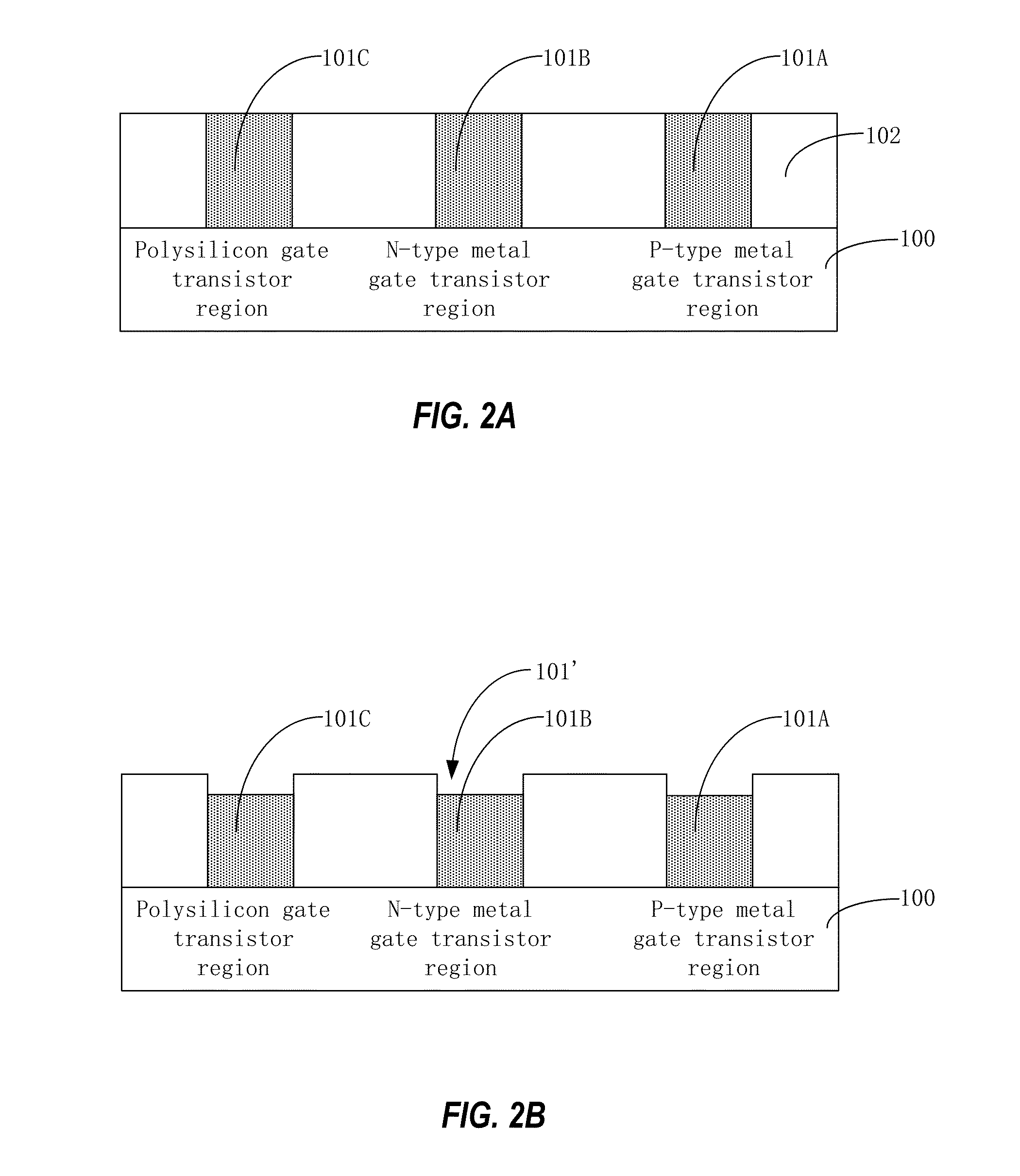
[0040]Step A1: provide a semiconductor substrate 100 comprising a front-end device, the front-end device comprising a first dummy gate 101A in a P-type metal gate transistor region, a second dummy gate 101B in an N-type metal gate transistor region, and a polysilicon gate 101C in a polysilicon gate region; and form an interlayer dielectric layer 102 on the semiconductor substrate, as shown in FIG. 2A.

[0041]In the embodiment, the front-end device is referred to as a structure that has been formed on the semiconductor substrate and may contain certain components, but th...

embodiment 2

[0072]FIG. 3 is a simplified flow chart of a method 300 for manufacturing a semiconductor device according to an embodiment of the present invention. Method 300 may include:

[0073]S101: provide a semiconductor substrate comprising a front-end device, the front-end device comprising a first dummy gate in a first type metal gate transistor region, a second dummy gate in a second type metal gate transistor region, and a polysilicon gate in a polysilicon gate transistor region; form an interlayer dielectric layer on the semiconductor substrate;

[0074]S102: remove by etching a thickness of the first dummy gate, a thickness of the second dummy gate, and a thickness of the polysilicon gate so that the first dummy gate, the second dummy gate, and the polysilicon gate are below the surface of the interlayer dielectric layer;

[0075]S103: form a protective layer on the first dummy gate, the second dummy gate, and the polysilicon gate;

[0076]S104: remove by etching a portion of the protective layer...


PUM

PropertyMeasurementUnit
timeaaaaaaaaaa
thicknessaaaaaaaaaa
thicknessaaaaaaaaaa

Abstract

A method for manufacturing a semiconductor device includes providing a substrate containing a front-end device and forming a dielectric layer on the substrate. The front-end device includes a first dummy gate in a first type metal gate transistor region, a second dummy gate in a second type metal gate transistor region, and a polysilicon gate in a polysilicon gate region. The method also includes removing a thickness of the first, second, and polysilicon gates and forming a protective layer on the polysilicon layer to protect the polysilicon layer during a CMP process, thereby improving the performance and yield of the semiconductor device.

Description

CROSS-REFERENCES TO RELATED APPLICATIONS[0001]This application claims priority to Chinese patent application No. 2014101226180.5, filed on May 26, 2014, the content of which is incorporated herein by reference in its entirety.BACKGROUND OF THE INVENTION[0002]The present invention relates to semiconductor devices and the fabrication of semiconductor devices, and more particularly to semiconductor devices in 32 nm technology nodes and beyond.[0003]In the field of semiconductor technology, aluminum or aluminum alloy is mainly used in high-k metal gate (HKMG) process technology nodes at 32 nm and below (e.g., 28 nm). The use of aluminum or aluminum alloy for metal gate electrodes has cost and performance advantages. The aluminum gate chemical mechanical polishing (CMP) process is a very important process for manufacturing high-k metal gate transistors with aluminum gates.[0004]In order to increase the gap filling space, a CMP process of aluminum gate structures typically includes two CM...

Claims


Application Information

Patent Timeline
Patent Type & Authority Applications(United States)
IPC IPC(8): H01L29/40H01L21/306H01L21/28H01L29/78H01L29/66H01L29/49
CPCH01L29/408H01L29/66545H01L21/30625H01L21/28035H01L29/7831H01L29/4916H01L21/82345H01L21/823456H01L21/28079H01L21/28123H01L21/3212
Inventor ZHAO, JIANWANG, HANGPING
Owner SEMICON MFG INT (SHANGHAI) CORP
Why Eureka
Try Eureka