Mask set and method for fabricating semiconductor device by using the same

a mask set and semiconductor technology, applied in the field of memory devices, can solve the problems of inferior performance, gate capacitance reduction, conventional polysilicon gate, etc., and achieve the effect of reducing the influence of alignment mismatch on fabrication processes

Active Publication Date: 2015-12-03
UNITED MICROELECTRONICS CORP
View PDF10 Cites 24 Cited by
  • Summary
  • Abstract
  • Description
  • Claims
  • Application Information

AI Technical Summary

Benefits of technology

[0009]One feature of the present disclosure is that portions of the serpentine pattern are disposed more away from the ends of the gate structures than other portions of the serpentine pattern. If there is an alignment mismatch which causes the shift of the serpentine pattern, a buffer region provided by the inwardly curved portions may be used to reduce the influence of this alignment mismatch on fabrication processes. Therefore, a work function metal layer in a first region may still be removed completely even if there is an alignment mismatch of the serpentine pattern.

Problems solved by technology

On the other hand, the conventional polysilicon gate also has faced problems such as inferior performance due to boron penetration and unavoidable depletion effect which increases equivalent thickness of the gate dielectric layer, reduces gate capacitance, and worsens a driving force of the devices.

Method used


Image

  • Mask set and method for fabricating semiconductor device by using the same
  • Mask set and method for fabricating semiconductor device by using the same
  • Mask set and method for fabricating semiconductor device by using the same

Examples


Embodiment Construction

[0024]In the following description, numerous specific details are given to provide a thorough understanding of the invention. It will, however, be apparent to one skilled in the art that the invention may be practiced without these specific details. Furthermore, some well-known system configurations and process steps are not disclosed in detail, as these should be well-known to those skilled in the art.

[0025]Likewise, the drawings showing embodiments of the apparatus are not to scale and some dimensions are exaggerated for clarity of presentation. Also, where multiple embodiments are disclosed and described as having some features in common, like or similar features will usually be described with same reference numerals for ease of illustration and description thereof.

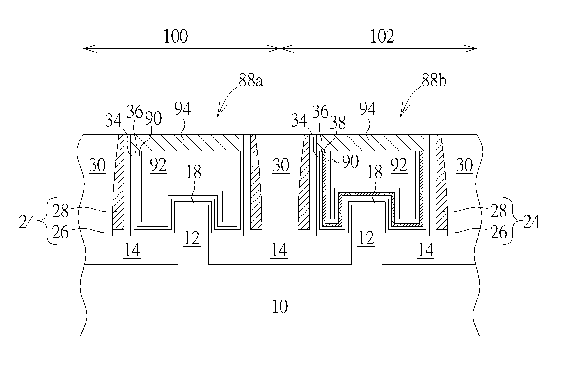
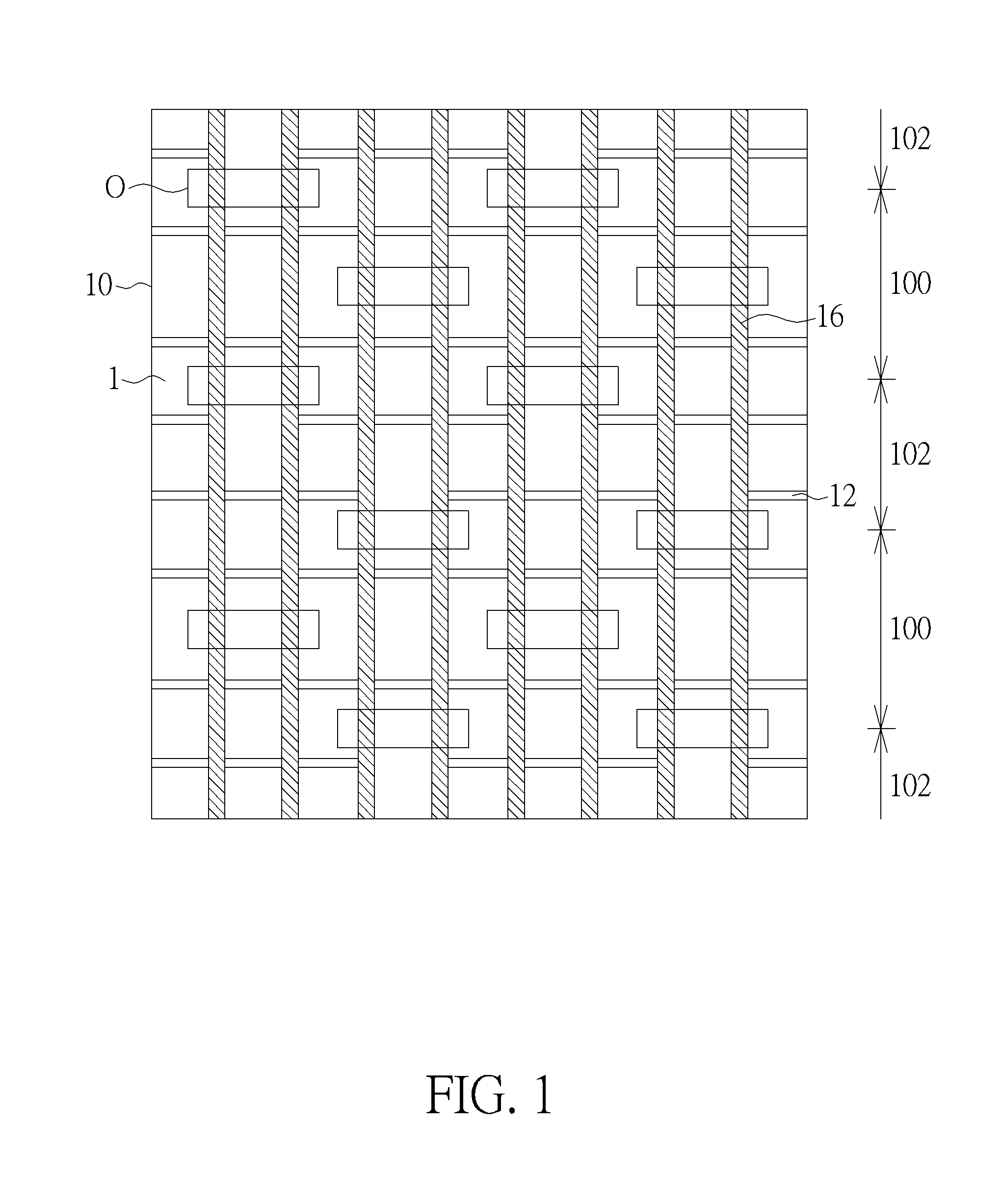
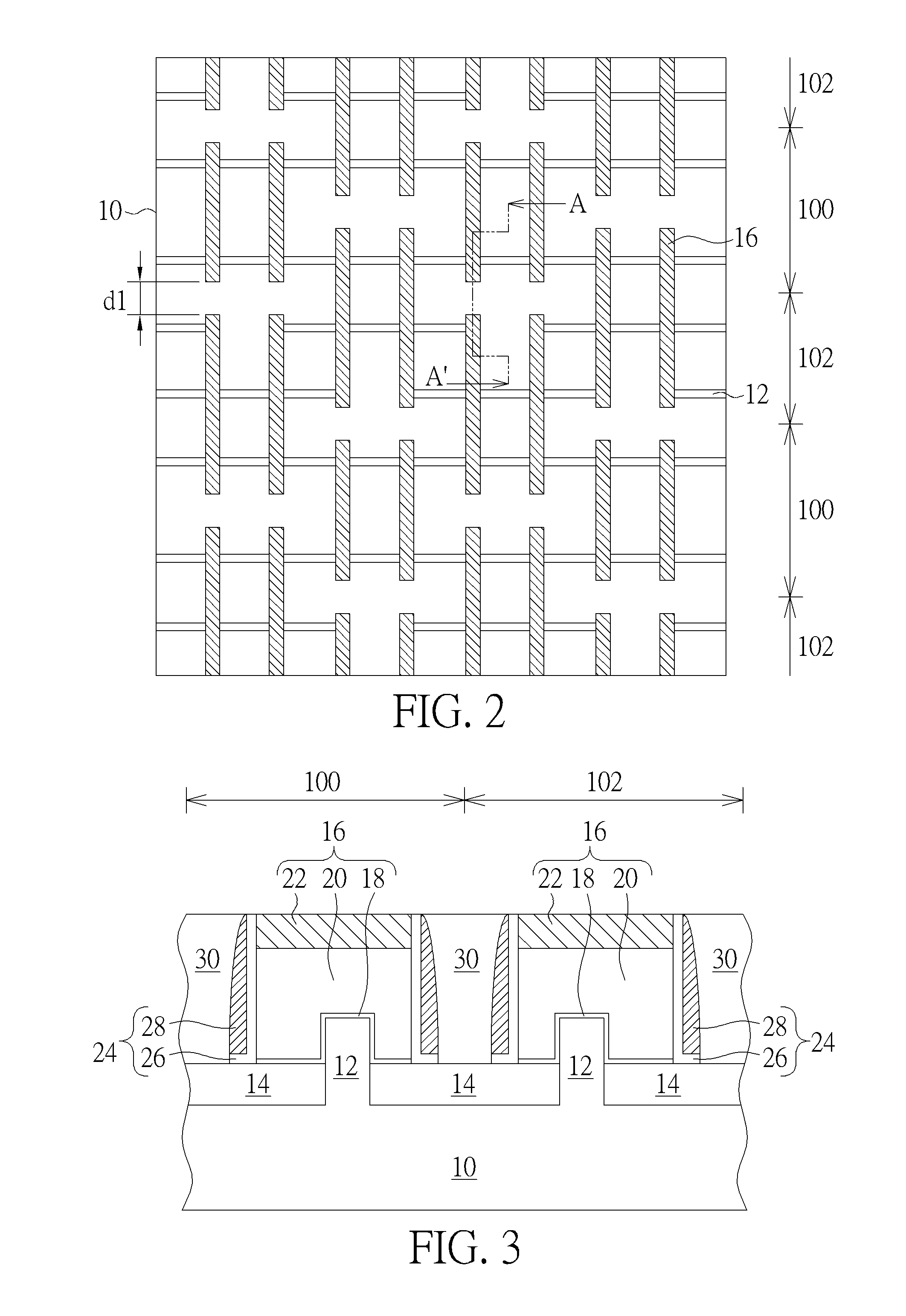
[0026]Please refer to FIG. 1. FIG. 1 is a schematic top view showing a semiconductor device at the beginning of the fabrication process. A substrate 10 having fin structures 12 is provided. Stripe-shaped gate structure...


PUM

PropertyMeasurementUnit
widthaaaaaaaaaa
distanceaaaaaaaaaa
lengthaaaaaaaaaa

Abstract

A mask set includes a first mask and a second mask. The first mask includes geometric patterns. The second mask includes at least a strip-shaped pattern with a first edge and a second edge opposite to the first edge. The strip-shaped pattern has a centerline along a long axis of the strip-shaped pattern. The first edge includes inwardly displaced segments shifting towards the centerline and each of the inwardly displaced segments overlaps each of the geometric patterns.

Description

BACKGROUND OF THE INVENTION[0001]1. Field of the Invention[0002]The present invention relates generally to the field of memory devices, and more particularly to a mask set used to fabricate memory devices and a method for fabricating semiconductor devices by using the mask set.[0003]2. Description of the Prior Art[0004]In the past few decades, semiconductor devices have become more and more integrated and methods used to fabricate the semiconductor devices have been improved continuously. Among all of the factors relevant to the electrical properties of the semiconductor devices, the thickness and dielectric constant of the gate dielectric layer are the most influential ones. In detail, in order to keep or enhance the drift current in the semiconductor devices, high dielectric constant (hereinafter abbreviated as high-k) materials are often used to replace the conventional silicon oxide as the gate dielectric layer. The main advantage of adopting the high-k materials is that it decr...

Claims


Application Information

Patent Timeline
Patent Type & Authority Applications(United States)
IPC IPC(8): H01L21/8238G03F1/00
CPCG03F1/00H01L21/823842
Inventor LEE, WEI-CHIWANG, YU-LINLEE, CHUNG-YUAN
Owner UNITED MICROELECTRONICS CORP
Why Eureka
Try Eureka