Semiconductor device having fin-shaped structure and method for fabricating the same

a technology of semiconductor devices and fins, applied in the direction of semiconductor devices, basic electric elements, electrical equipment, etc., can solve the problems of bottlenecks in conventional finfet fabrication of utilizing epitaxial materials and increasing carrier mobility

Active Publication Date: 2015-12-10
MARLIN SEMICON LTD
View PDF2 Cites 14 Cited by
  • Summary
  • Abstract
  • Description
  • Claims
  • Application Information

AI Technical Summary

Benefits of technology

[0007]According to a preferred embodiment of the present invention, a method for fabricating semiconductor device with fin-shaped structure is disclosed. The method includes the steps of: forming a fin-shaped structure on a substrate; forming a first dielectric layer on the substrate and the fin-shaped structure; depositing a second dielectric layer on the first dielectric layer; etching back a portion of the second dielectric layer; removing part of the first dielectric layer to expose a top surface and part of the sidewall of the fin-shaped structure; forming an epitaxial layer for covering the exposed top surface and part of the sidewall of the fin-shaped structure; and removing a portion of the second dielectric layer.

Problems solved by technology

Nevertheless, conventional FinFET fabrication of utilizing epitaxial materials such as silicon germanium to increase carrier mobility has reached a bottleneck.

Method used


Image

  • Semiconductor device having fin-shaped structure and method for fabricating the same
  • Semiconductor device having fin-shaped structure and method for fabricating the same
  • Semiconductor device having fin-shaped structure and method for fabricating the same

Examples


Embodiment Construction

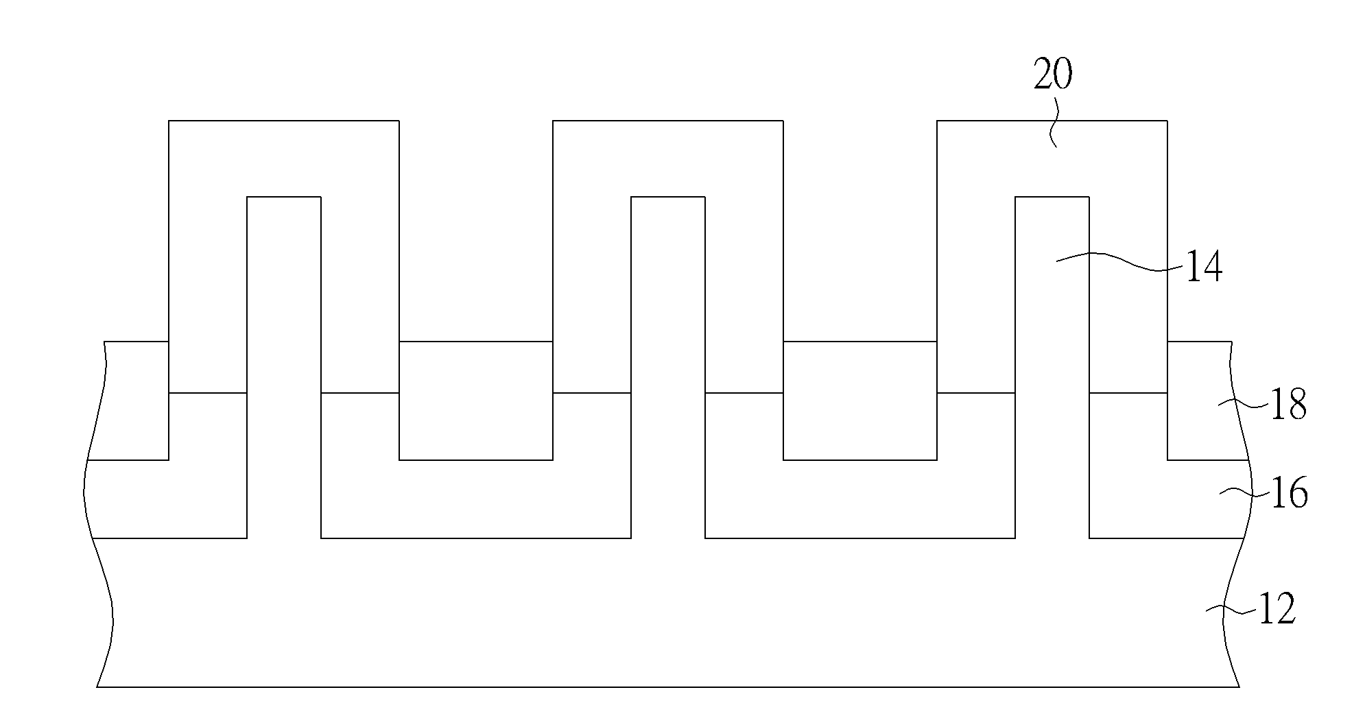
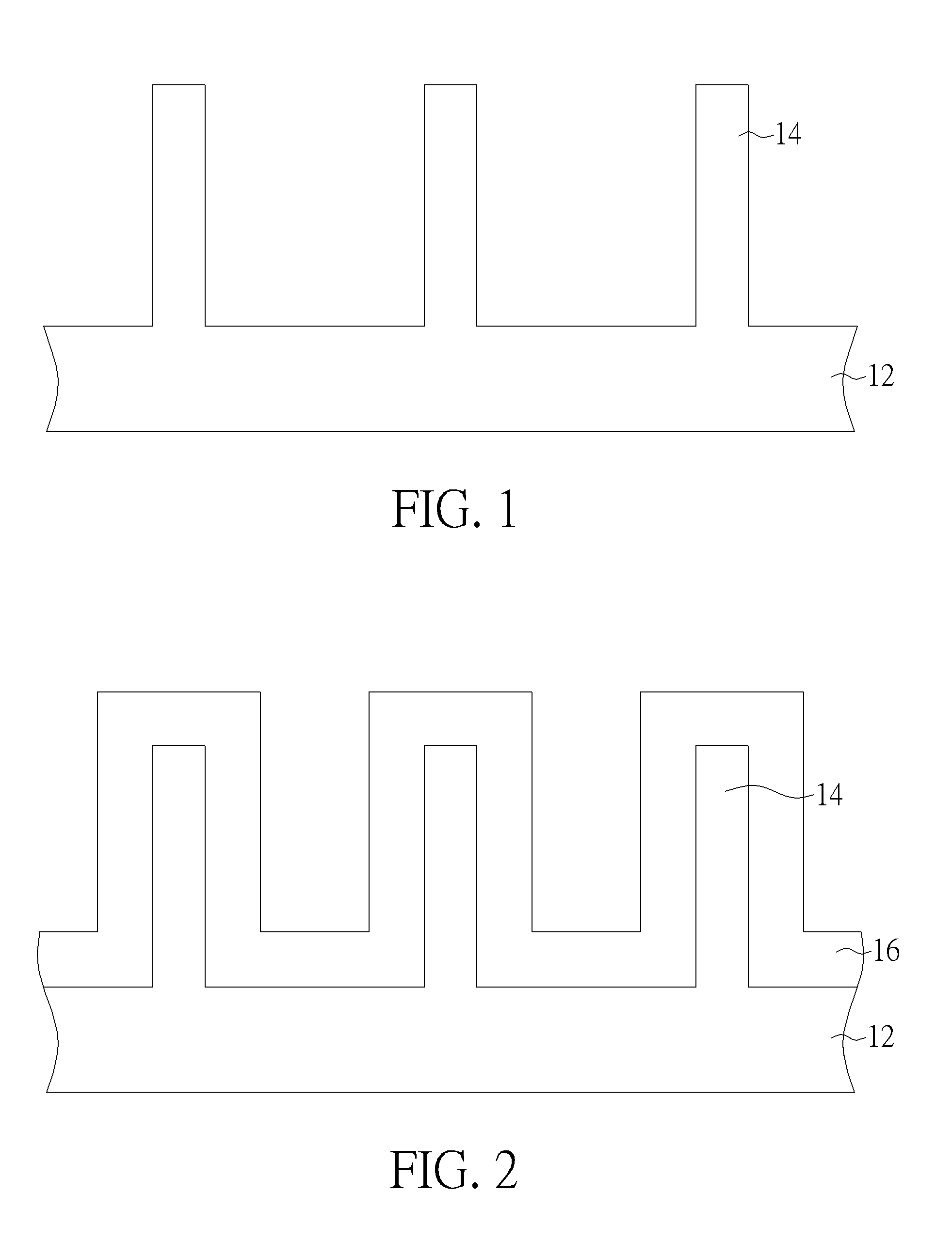
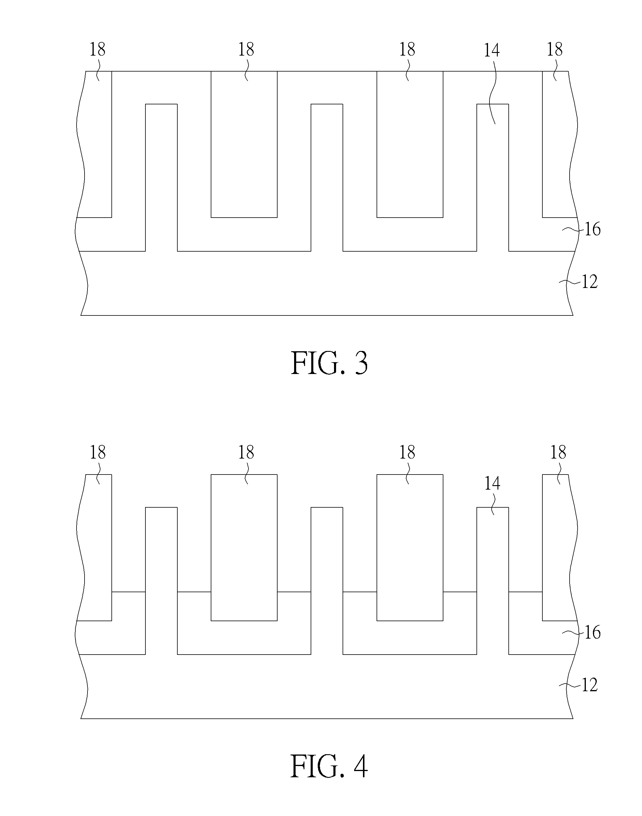
[0011]Referring to FIGS. 1-7, FIGS. 1-7 illustrate a method for fabricating semiconductor device according to a preferred embodiment of the present invention. As shown in FIG. 1, a substrate 12, such as a silicon substrate or silicon-on-insulator (SOI) substrate is first provided, and at least one fin-shaped structure 14 is formed on the substrate 12. It should be noted that even though three fin-shaped structures 14 are disclosed in this embodiment, the quantity of the fin-shaped structures 14 is not limited to three, but could be any quantity greater than one.

[0012]In addition, the fin-shaped structures 14 of this embodiment are preferably obtained by a sidewall image transfer (SIT) process. For instance, a layout pattern is first input into a computer system and is modified through suitable calculation. The modified layout is then defined in a mask and further transferred to a layer of sacrificial layer on a substrate through a photolithographic and an etching process. In this wa...


PUM


Abstract

A semiconductor device with fin-shaped structure is disclosed. The semiconductor device includes: a substrate; a fin-shaped structure on the substrate; and an epitaxial layer on a top surface and part of the sidewall of the fin-shaped structure, in which the epitaxial layer and the fin-shaped structure includes a linear gradient of germanium concentration therebetween.

Description

BACKGROUND OF THE INVENTION[0001]1. Field of the Invention[0002]The invention relates to a semiconductor device having fin-shaped structure, and more particularly, to a semiconductor device with epitaxial material wrapped around fin-shaped structure.[0003]2. Description of the Prior Art[0004]In recent years, as various kinds of consumer electronic products have continuously improved and been miniaturized, the size of semiconductor components has reduced accordingly, in order to meet requirements of high integration, high performance, and low power consumption.[0005]With the trend in the industry being towards scaling down the size of the metal oxide semiconductor (MOS) transistors, three-dimensional or non-planar transistor technology, such as fin field effect transistor (FinFET) technology has been developed to replace planar MOS transistors. Since the three-dimensional structure of a FinFET increases the overlapping area between the gate and the fin-shaped structure of the silicon...

Claims


Application Information

Patent Timeline
Patent Type & Authority Applications(United States)
IPC IPC(8): H01L21/02H01L29/36H01L29/78H01L21/311
CPCH01L21/02532H01L21/31111H01L29/36H01L29/0657H01L29/7853H01L29/06H01L29/785H01L29/7848H01L29/1054H01L21/30604H01L21/0228H01L29/66795
Inventor CHIEN, CHIN-CHENGHSU, HSIN-KUOLIU, CHIH-CHIENLIN, CHIN-FUWU, CHUN-YUAN
Owner MARLIN SEMICON LTD
Why Eureka
Try Eureka