Conductive substrate and method for manufacturing same
a technology of conducting substrate and manufacturing method, which is applied in the manufacture of final products, resistive material coatings, organic semiconductor devices, etc., can solve the problems of increasing the price of the substrate, the method is not a reasonable method, etc., and achieves the effect of reducing resistance loss, simple process, and efficient conducting substra
- Summary
- Abstract
- Description
- Claims
- Application Information
AI Technical Summary
Benefits of technology
Problems solved by technology
Method used
Image
Examples
example 1
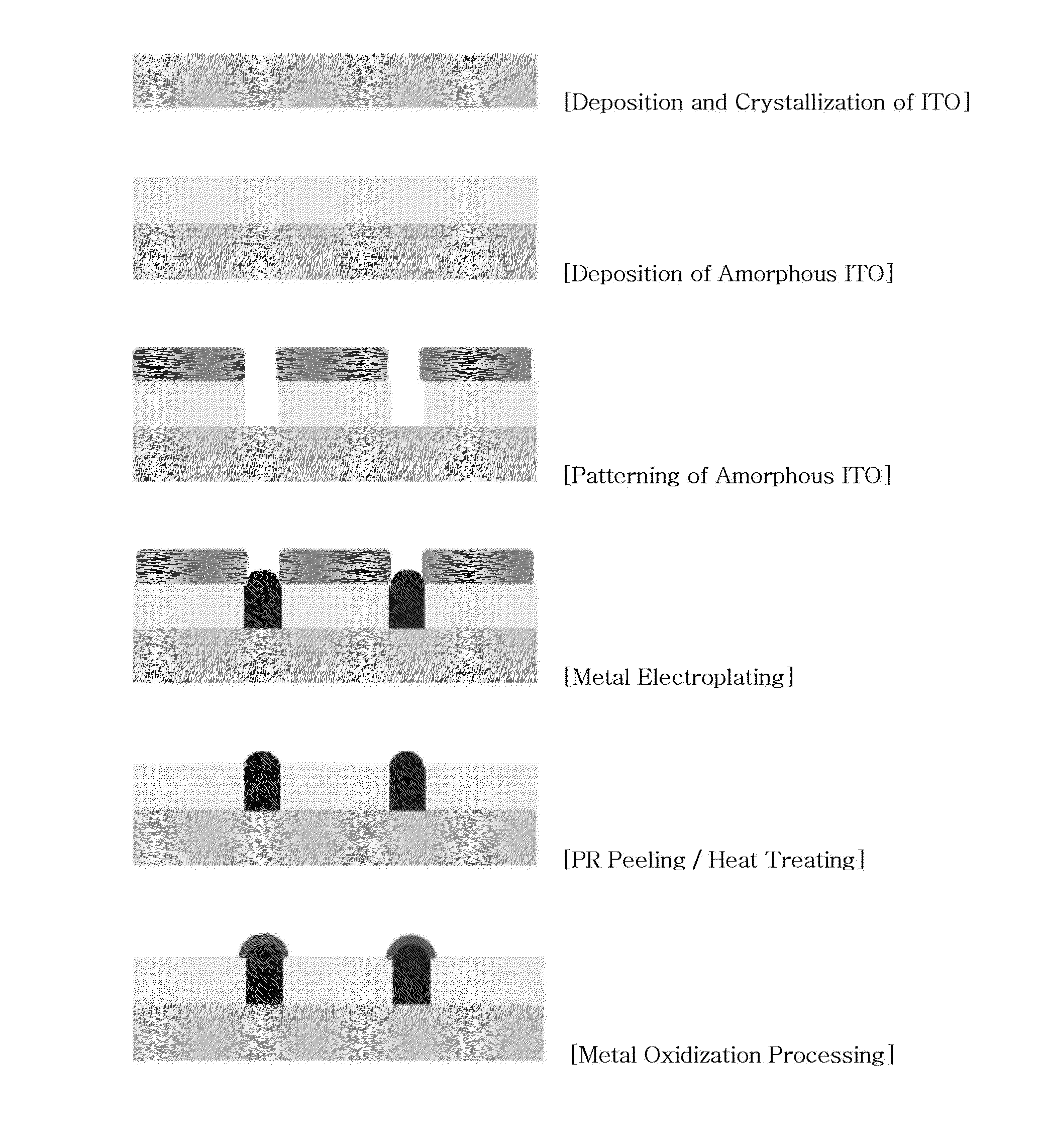
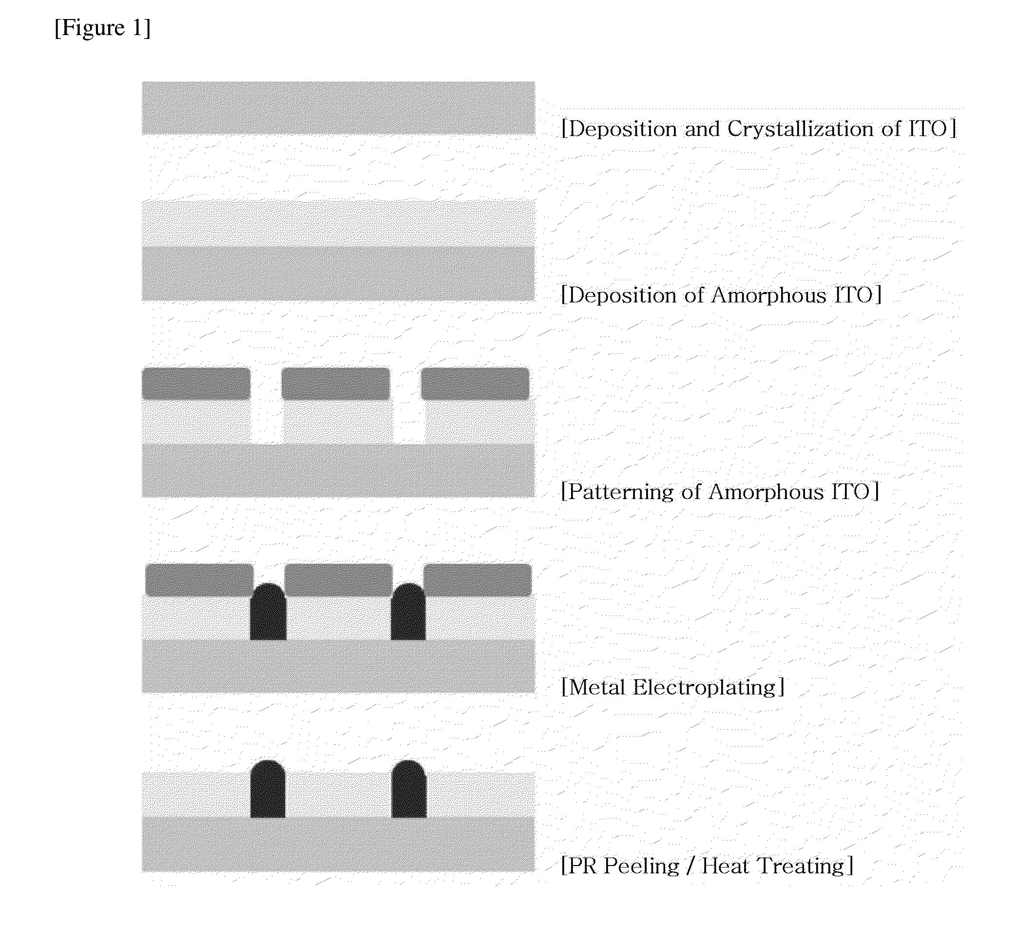
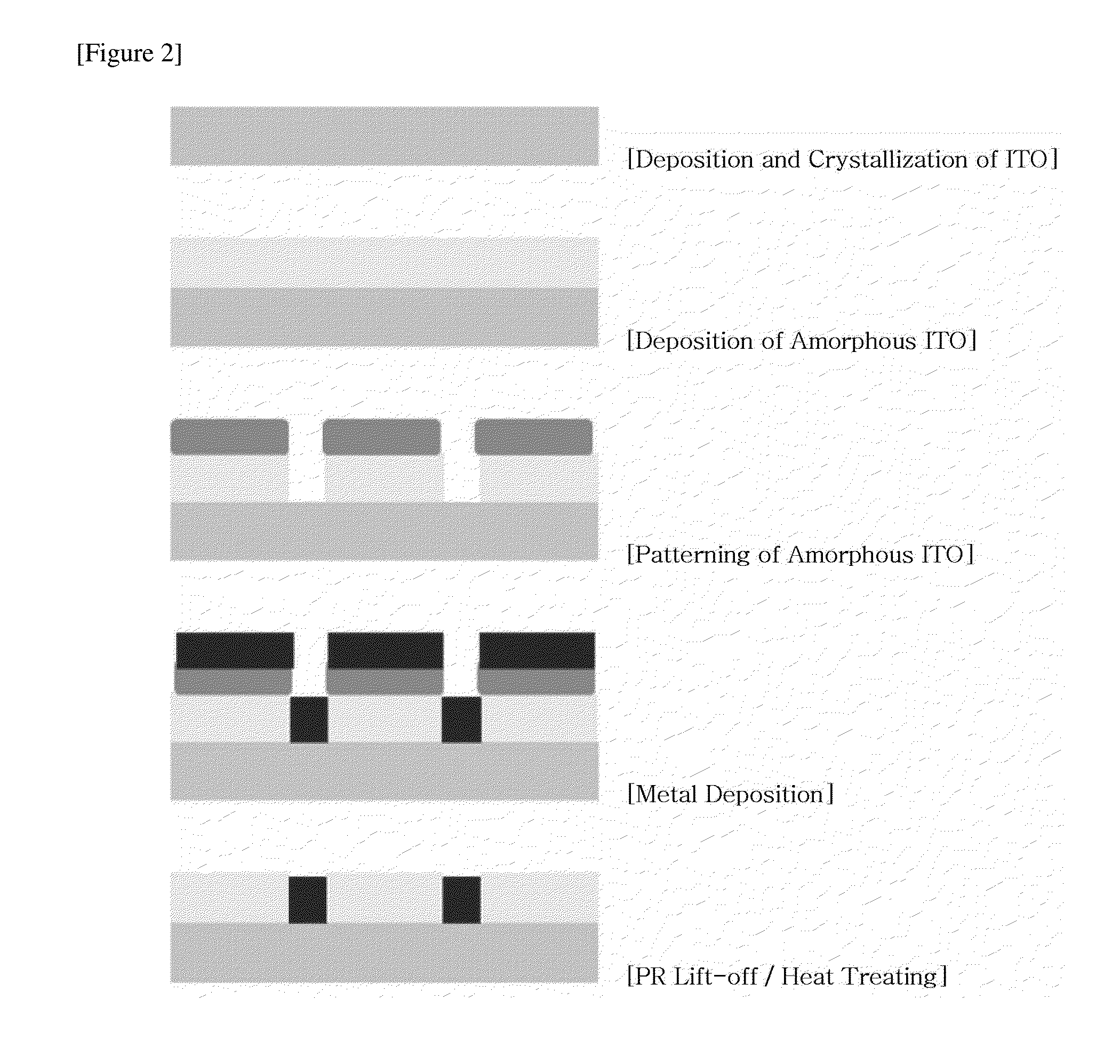
1) Forming Crystalline Transparent Conducting Layer on Glass Substrate
[0084]A crystalline indium tin oxide (ITO) thin film having a thickness of 300 nm was formed on a glass substrate by using materials and conditions described below. Specific resistance of the prepared crystalline ITO thin film was 2×10⁻⁴ Ωcm.
[0085]Deposition temperature: 400° C. (using RF Magnetron sputter)
[0086]Target: In2O3:SnO2=90 mol %:10 mol % purity 99.99% (Cerac Co)
[0087]RF Power: 150 W
[0088]Deposition Conditions: deposition time (30 min), pressure (10 mtorr)
[0089]Post heat treatment: 400° C. for 1 min
2) Forming Amorphous Transparent Conducting Layer on Crystalline Transparent Conducting Layer
[0090]An amorphous ITO thin film having a thickness of 300 nm was formed on a crystalline ITO thin film by using materials, equipment, and conditions below. Specific resistance of the prepared amorphous ITO thin film was 10×10−4 Ωcm.
[0091]Deposition temperature: 110° C. (using RF Magnetron sputter)
[0092]Target: In2O3:S...
example 2
[0098]After the metal electroplating according to Example 1 above, a metal oxide layer was formed by heat treatment at 500° C. for approximately 30 min under an oxygen atmosphere by using RTA equipment through electroless plating.
[0099]According to exemplary embodiments of the present invention, an efficient conducting substrate can be formed by a simple process. Further, in the present invention, an amorphous transparent conducting layer and a metal layer are introduced to minimize resistance loss of a crystalline transparent conducting layer.
[0100]Further, according to exemplary embodiments of the present invention, since the conducting substrate can be prepared without introducing an additional insulating layer formed on a secondary substrate in the related art, the number of processes can be reduced, and as a result, the competitive price can be secured.
PUM
| Property | Measurement | Unit |
|---|---|---|
| glass transition temperature | aaaaa | aaaaa |
| Tg | aaaaa | aaaaa |
| transparent | aaaaa | aaaaa |
Abstract
Description
Claims
Application Information


