Data bus inversion usable in a memory system

a data bus and memory system technology, applied in error detection/correction, redundant data error correction, instruments, etc., can solve problems such as power draw, data bus is susceptible to cross talk, simultaneous switching noise, intersymbol interference,

Active Publication Date: 2015-12-17
MICRON TECH INC
View PDF5 Cites 9 Cited by
  • Summary
  • Abstract
  • Description
  • Claims
  • Application Information

AI Technical Summary

Problems solved by technology

As discussed in U.S. patent application Ser. No. 11 / 873,779, filed Oct. 17, 2007, a data bus is susceptible to cross talk, simultaneous switching noise, intersymbol interference, and draws power based on the state of the data and / or frequency of data transition.

Method used


Image

  • Data bus inversion usable in a memory system
  • Data bus inversion usable in a memory system
  • Data bus inversion usable in a memory system

Examples


Embodiment Construction

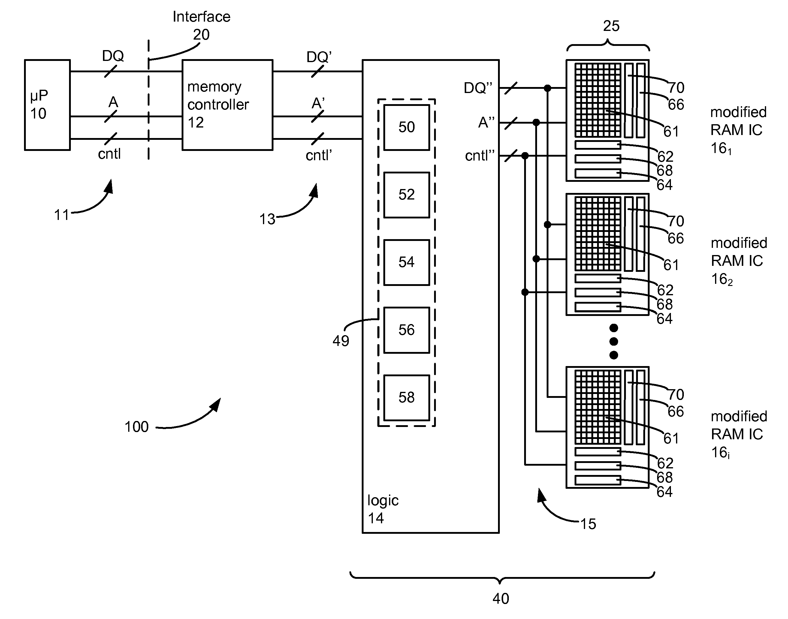
[0018]Implementations of Data Bus Inversion (DBI) techniques within a memory system are disclosed. In one embodiment, a set of random access memory (RAM) integrated circuits (ICs) is separated from a logic system by a bus. The logic system can contain many of the logic functions traditionally performed on conventional RAM ICs, and accordingly the RAM ICs can be modified to not include such logic functions. The logic system, which can be a logic integrated circuit intervening between the modified RAM ICs and a traditional memory controller, additionally contains DBI encoding and decoding circuitry. In such a system, data is DBI encoded and at least one DBI bit issued when writing to the modified RAM ICs. The RAM ICs in turn store the DBI bit(s) with the encoded data. When the encoded data is read from the modified RAM ICs, it is transmitted across the bus in its encoded state along with the DBI bit(s). The logic integrated circuit then decodes the data using the DBI bit(s) to return ...


PUM


Abstract

Implementations of Data Bus Inversion (DBI) techniques within a memory system are disclosed. In one embodiment, a set of random access memory (RAM) integrated circuits (ICs) is separated from a logic system by a bus. The logic system can contain many of the logic functions traditionally performed on conventional RAM ICs, and accordingly the RAM ICs can be modified to not include such logic functions. The logic system, which can be a logic integrated circuit intervening between the modified RAM ICs and a traditional memory controller, additionally contains DBI encoding and decoding circuitry. In such a system, data is DBI encoded and at least one DBI bit issued when writing to the modified RAM ICs. The RAM ICs in turn store the DBI bit(s) with the encoded data. When the encoded data is read from the modified RAM ICs, it is transmitted across the bus in its encoded state along with the DBI bit(s). The logic integrated circuit then decodes the data using the DBI bit(s) to return it to its original state.

Description

FIELD OF THE INVENTION[0001]Embodiments of this invention relate to implementation of data bus inversion in a memory system.BACKGROUND[0002]An example illustrating data transmission between high-speed components within a single semiconductor device, or between two devices on a printed circuit board, is represented by the system 1 shown in FIG. 1. In FIG. 1, a transmitter 2 (e.g., a microprocessor) sends data over one or more transmission channels 4x (e.g., conductive traces “on-chip” in a semiconductor device or on a printed circuit board) to a receiver 6 (e.g., another microprocessor or memory). As a group, such transmission channels 4x are often referred to as a “data bus,” which allows one or more data signals to be transmitted from one device to another.[0003]As discussed in U.S. patent application Ser. No. 11 / 873,779, filed Oct. 17, 2007, a data bus is susceptible to cross talk, simultaneous switching noise, intersymbol interference, and draws power based on the state of the da...

Claims


Application Information

Patent Timeline
Patent Type & Authority Applications(United States)
IPC IPC(8): G06F11/10
CPCG06F11/1048G06F11/1004G06F11/1008
Inventor HOLLIS, TIMOTHY M.
Owner MICRON TECH INC
Why Eureka
Try Eureka